PILOT-NX-V8-HF-UK
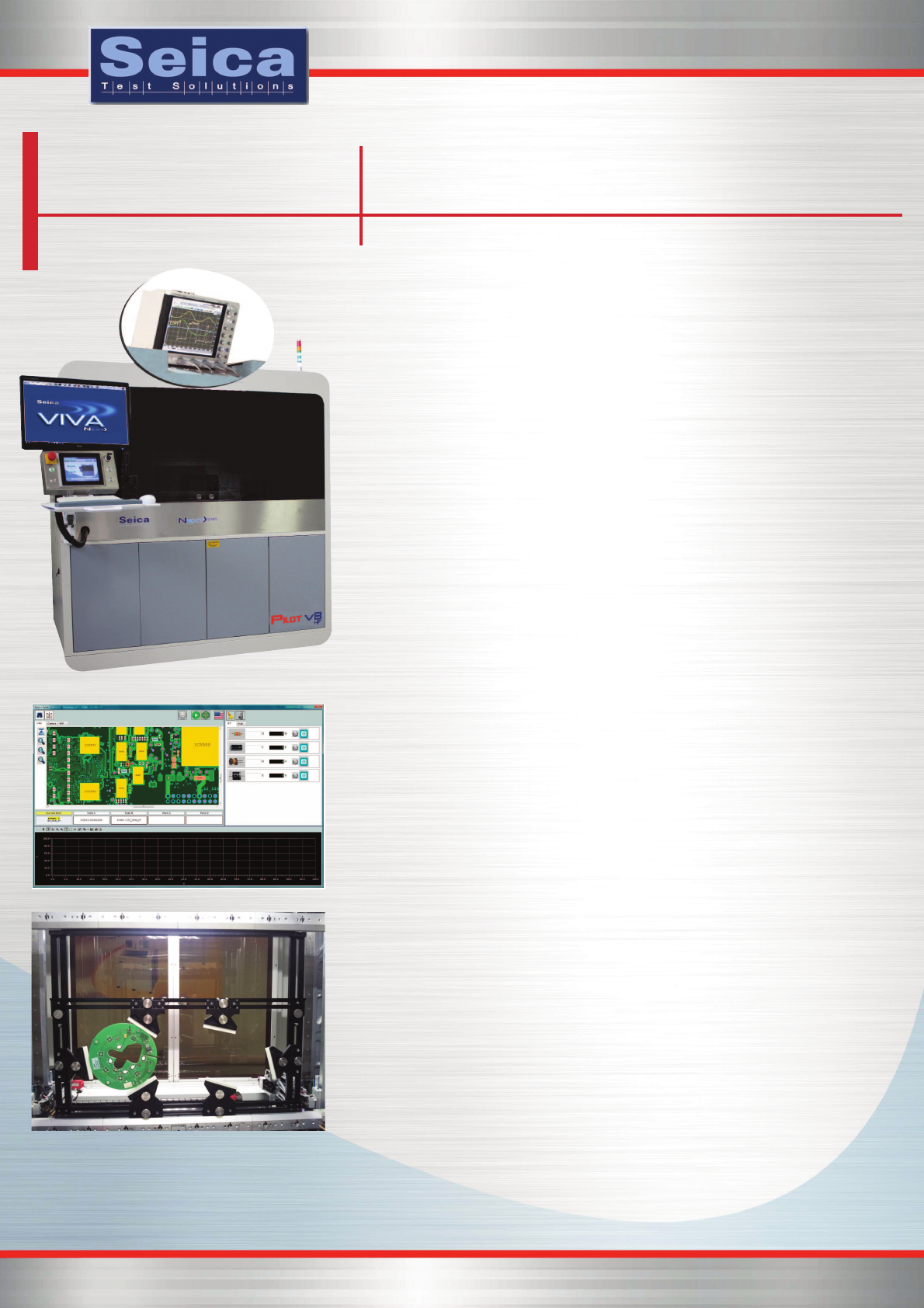
F L Y I N G P R O B E S Y S T E M PILOT V8 HF N EXT > S ERIES PILOT N EXT > S ERIES LINE Current electronics trend shows a major direction for the board production: min iat uri zat ion . Mor e pro duc ts ha ve no w…
FLYING PROBE SYSTEM
PILOT V8
HF
NEXT>SERIES
PILOT NEXT>SERIES LINE
Current electronics trend shows a major direction for the board production:
miniaturization. More products have now very small dimensions and test
engineers have no possibility to allocate the necessary test points for the
validation. Today a new challenge is connected to this situation: the
requirement to test HF signals before final product assembly.
The solution for this application is the Flying probe technology, integrating
the high accuracy of positioning 8 probes on the UUT and the capability to
measure very high frequency signals.
Based on the consolidated and complete solution of the Seica Flying Probes
line, the
PILOT V8
HF
NEXT>SERIES includes the performance to test up
to 1.6 GHz and locate probes on 008004 pad size. The
PILOT V8
HF
NEXT>SERIES vertical architecture is the optimum solution for probing both
sides of the UUT simultaneously. This increases test accessibility and flexibility,
while guarantees fast, precise, reliable and repeatable probing: full availability of
all the mobile resources for testing the UUT. This solution represents an important
technological innovation in double-sided flying probe test, overcoming the
intrinsic limitations of horizontal systems. The requirement for standard ICT &
Functional testing of the DUT is still part of the basic requirement and is
realized using the Seica proprietary hardware, so that the implemented resources
are used for the DUT validation. All power supply, DUT enable signals, current
consumption control are realized with the 18 bit resolution ACL measuring card
and switching matrix which allows future expansion capabilities.
Flylab and National Instruments Software Tools
To make the solution easier to use, as an unique tool in the market, the
complete solution is driven by LabView
TM
/TestStand
TM
interface. Engineers
are now able to move probes on a specific target (down to 008004
components) and perform the highest definition test by using a graphical and
user-friendly SW interface. The Flying Probe system still integrates Seica
native capabilities but can be completely driven by LabView
TM
functionalities
and makes the technology available for all NI software users to implement
new and additional features. All system resources are open and easy to
manage. The DUT functionality can be tested under critical environmental
conditions: the ability to implement a thermal stress test (from 0° to 70°C)
is reached integrating a cooling and heating system in the testing area.
Managed frequency can be implemented to reach the coverage of BT and
WI-FI ranges to make the solution ever more performing.
The test tools and techniques include:
• FNODE signature analysis on the nets of the UUT
• Standard analog and digital in-circuit test
• Vectorless tests (JSCAN and OPENFIX), to test ICs for opens and shorts
• PWMON net analysis for power on the boards
• Continuity test to detect open tracks on the PCB
• Visual tests for component presence/absence and rotation
• Optional Thermal Scan Resources
• ALI: Automatic Laser Inspection for presence/absence and warpage
compensation
• Up to 4 HF channels with variable pitch ground probe
• Up to 1.6 GHz bandwidth with S-parameters compensation
• Up to 20 GSa/s depending of the instrument selected
• Active probe amplifier
TECHNICAL TABLE
SEICA WORLDWIDE
SEICA SpA
via Kennedy 24
10019 Strambino - TO
ITALY
Tel: +39 0125 6368.11
Fax: +39 0125 6368.99
Email: sales@seica.com
PROXIMA S.r.l.
Email: info@proxima-ate.com
SEICA Inc.
Email: dave.sigillo@seicausa.com
SEICA FRANCE SARL
Email: dupoux@seica.fr
SEICA DEUTSCHLAND GmbH
Email: marc.schmuck@seica.com
SEICA ELECTRONICS
(Suzhou) Co.Ltd.
Email: seicachina@seica.com
Seica reserves the right to change the
technical specifications without notice
TDS Pilot Next> series V8HF vers. 02 UK 05/2018
VIVA NEXT> is available in
a 32 and 64 bit version with a
new graphical interface and a
guided environment for an easy
and quick test program
creation. It is fully integrated
with NI-VISA drivers and with
third-party test management
software.
Probes Position - Test Side Front/Rear
Number of “ICT Test Probes” 4 (2 front, 2 rear)
Number of “High Frequency / Electrical Probes” 4 (2 front, 2 rear)
Number of Fixed Probes up to 192
Maximum Digital Embedded Channels 4
Thermal Scan Module (option) 2 (1 front, 1 rear)
Number of CCD HR 5Mpixel Colour Cameras 2 (1 front, 1 rear)
Number of CCD view probes Colour Cameras 2 (1 front, 1 rear)
Marker Recognition Automatic
UUT Planarity Compensation Automatic
Cooler and Heater system Optional
Board Clamping System Manual (Dual Action)
Active Test Area 560 x 480 mm (22.1 X 18.9")
Minimum Board Size (*) 20 x 20 mm (0.79 x 0.79")
Minimum Board Thickness 0.3 mm (0.0012")
Maximum Board Thickness 5 mm (0.19")
UUT Edge Clearance 2 mm
Universal Carrier (**) Optional
Minimum Pad Pitch 150 μm (6 mil) (***)
Minimum Pad Size 75 μm (3 mil)
XY axis resolution, brushless motor 2.5 μm (1 μm option)
Z-axis Travel -3.0 mm to 40 mm programmable
Z axis resolution, linear motor 1 µm
Contact Force 10 g – 100 g programmable
Voltage Generator 1 DC/AC (DRA) ±1 mV to ±10 V (±0.1%)
Voltage Generator 2 DC/AC (DRB) ±1 mV to ±10 V (±0.1%)
Voltage Generator 3 DC/AC (DRC) ±25 mV to ±100 V (±0.2%)
Current Generator DC/AC ±1 nA to ±0.5 A (±0.1%)
Waveform Generator 1 Sin, Tri, Arbitrary (DRA) 1 Hz to 3 MHz (±1 mHz ) - ±10 V max
Waveform Generator 2 Sin, Tri, Arbitrary (DRC) 1 Hz to 10 KHz (±10 mHz ) - ±100 Vmax
Voltage Measurements DC/AC ±200 μV to ±100 V
Current Measurements DC/AC ±3 nA to ±0.5 A
Frequency Measurement 0.1 Hz to 50 MHz
Digital Embedded Channel ±12 V - 500 mA - 10 MHz
Resistance Measurement 1 mΩ to 100 MΩ
Capacitance Measurement 1 pF to 1 F
Inductor Measurement 1 μH to 1 H
Zener Measurement up to 100 V (200V option)
Automatic Visual Inspection
Bandwidth up to 1.6 GHz (based on selected instrument)
Sampling rate up to 20 GSa/s (based on selected instrument)
Temperature Range 23°C ± 5°C
Humidity 30 - 80 %
Power Consumption 3.5 kW max 1.0 kW max
Air Flow 0.35 CFM – 10 l/min. 0.3 CFM – 6 l/min.
Weight 1400 kg (3086 Ibs)
Depth 1265 mm (49.8”) 2165 mm open doors (85.3”)
Width 1750 mm (68.9”) 3374 mm open doors (132.8”)
Height 1800 mm (70.9”) 2230 mm (87.8”) with light-tower
PC/Operating System Windows 10
Software VIVA NEXT
Automatic Test Generation Yes
Autodebug Yes
Data Input Format CAD Data/Manual
Parallel Test Capabilities Yes
* Universal carrier for unique board configurations.
** for clamping not-regular shape PCB.
*** With limited numer of probes.