265ProFlow.pdf - 第29页
TECHNI CAL REFEREN CE ELECTRICAL DETAIL Chapter Issue 8 Dec 02 ProFlow Manual 1.25 ELECTRICAL DET AIL For electrica l detai l on Infinit y , Horizon and ELA machines refer to the respecti ve T echnical Reference manual .…
TECHNICAL REFERENCE
MECHANICAL DETAIL
1.24 ProFlow Manual Chapter Issue 8 Dec 02
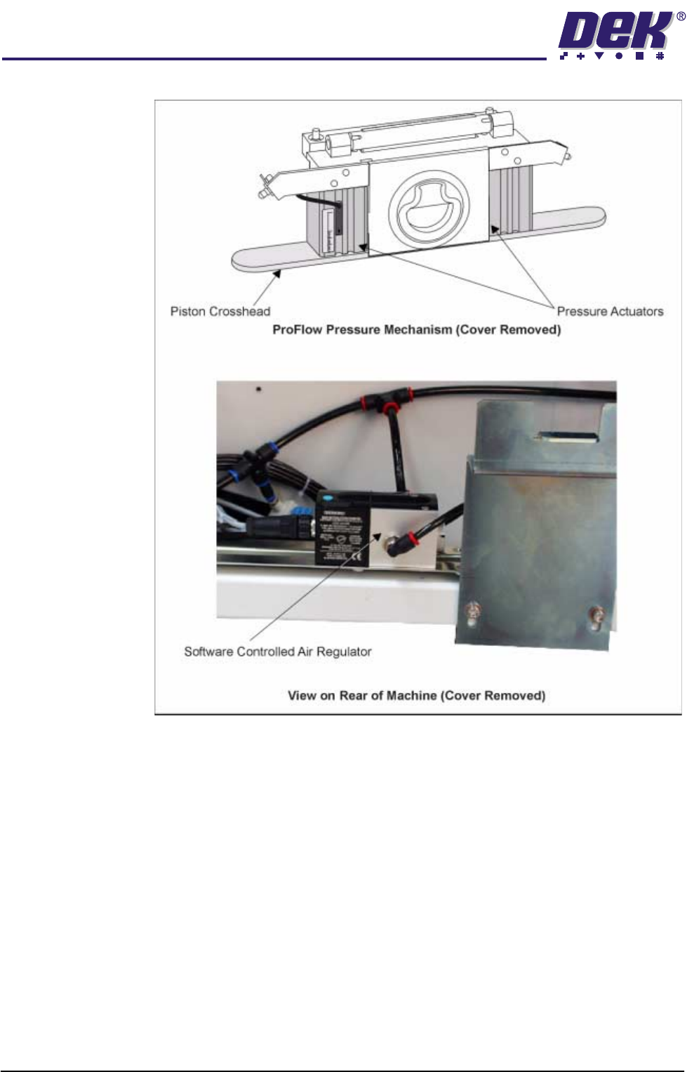
Figure 1-18 Software Controlled Pressure Mechanism - Norgren
TECHNICAL REFERENCE
ELECTRICAL DETAIL
Chapter Issue 8 Dec 02 ProFlow Manual 1.25
ELECTRICAL DETAIL
For electrical detail on Infinity, Horizon and ELA machines refer to the
respective Technical Reference manual. For GSX and Lt machines only, a
PCADADIO card is used. The PCADADIO card is a multi-purpose I/O board
with the following functions:
• 8 Differential Multiplexed Analogue Inputs.
• Two Analogue Outputs.
• 16 Digital I/Os.
• 3 Counter-timer Channels.
The operation of these functions are controlled using the PC XT bus and link
options.
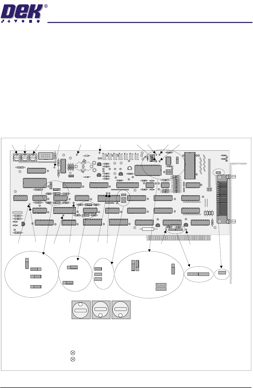
Figure 1-19 PCADADIO Card Layout
1 1 1
TP13 TP10 TP9 TP2 TP3TP5TP6
TP1TP4TP12
TP7TP8
TP14 TP15
TP11
SW1 SW2 SW3
1
8 8
PCADADIO, ENCLOSURE Y3, CARD X3
RED
GREEN
Illuminates when board is accessed by processor.
Illuminates when board is in normal use.
Sets a unique board-slot address for PCIB40 #5 .
(I/0 addressing uses this base address to point to data channels).
SWITCH SW1 SW2 SW3
8
1
8
THIS BOARD SLOT POSITION =
SW
1
SW
2
SW
3
LK14
B
B
A
A
BA
LK15
B
A
LK16
LK17
LK13
A
B
LK12
A
B
LK9
LK10
LK11
LK6
LK5
LK3
LK7
LK8
A
A
A
A
A
B
B
B
B
B
LK1
LK2LK4
BAA
B
TECHNICAL REFERENCE
ELECTRICAL DETAIL
1.26 ProFlow Manual Chapter Issue 8 Dec 02
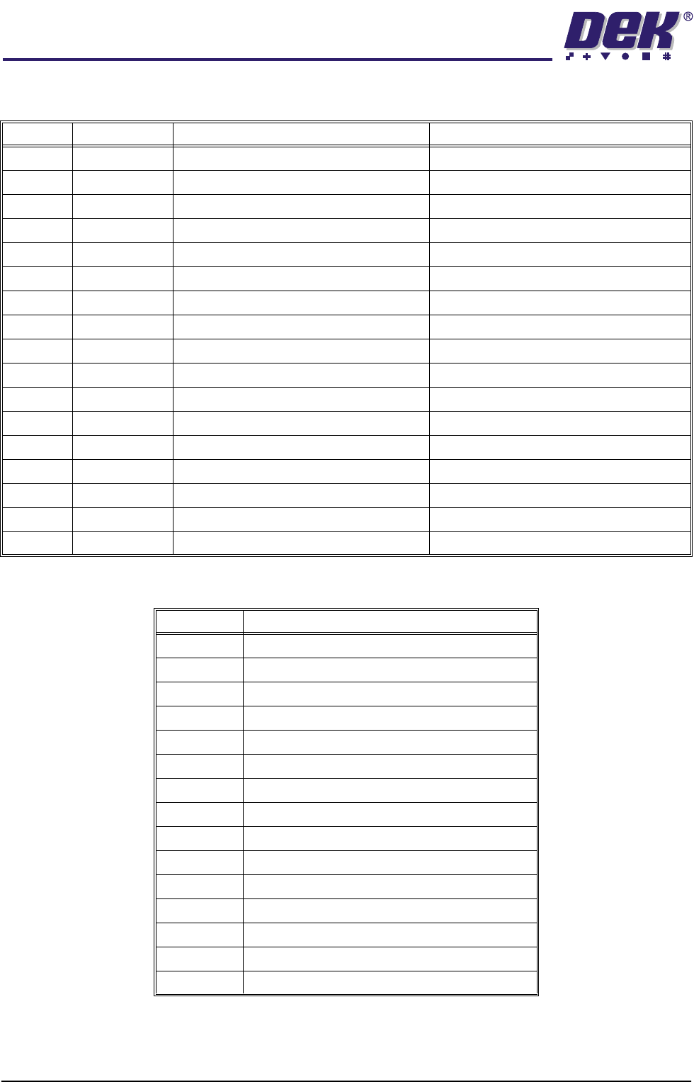
Jumper Link Functions
Test Points
Link Status Function Result
LK1 Omitted Pseudo Differential Ground Connection PCADADIOCD, different inputs
LK2 Omitted ADC Interrupt Selection Not Used
LK3 A Differential/Single-ended Input Selection PCADADIOCD
LK4 Omitted Counter/Timer Interrupt Selection Not Used
LK5 Omitted DAC1 Output Range 0V to 10V
LK6 Omitted DAC0 Output Range 0V to 10V
LK7 B ADC Input Range -10V - to +10V
LK8 A ADC Input Range -10V - to +10V
LK9 Fitted ADC Trigger Source Enable software triggering
LK10 Omitted ADC Trigger Source Disable hardware triggering
LK11 Omitted ADC Trigger Source Disable Counter/timer channel A triggering
LK12 B Digital I/O Reset State Digital I/O lines DIG0-3
LK13 B Digital I/O Reset State Digital I/O lines DIG4-75
LK14 B Digital I/O Reset State Digital I/O lines DIG8-11
LK15 B Digital I/O Reset State Digital I/O lines DIG12-15
LK16 B Counter/Timer Channel A Clock Sequence 1Mhz Clock
LK17 A Digital I/O Reset Test Link Automated board testing of the I/O’s
Test Point Function
TP1 PCbus IRQ2
TP2 DAC Voltage Reference
TP3 +5V Analogue
TP4 PCbus IRQ3
TP5 Analogue + Supply (Approx. 15V)
TP6 Analogue - Supply (Approx. - 15V)
TP7 ADC Chip Enable
TP8 ADC Status Line
TP9 Analogue Ground
TP10 Digital Ground
TP11 Buffered Reset Active Low
TP12 I/O Address Match
TP13 +5V Digital
TP14 Device Write Active Low
TP15 Device Read Active Low