VI User Manual.pdf - 第285页
2D solder paste inspection Vision 2007 4.10 User Manua l Rev 01 9 - 7 Bridge detection ( I ): the short circuit detec- tion feature can be activated by picking the op- tion Bridge detect ion . The short circuit detection…
2D solder paste inspection
9 - 6 Vision 2007 4.10 User Manual Rev 01
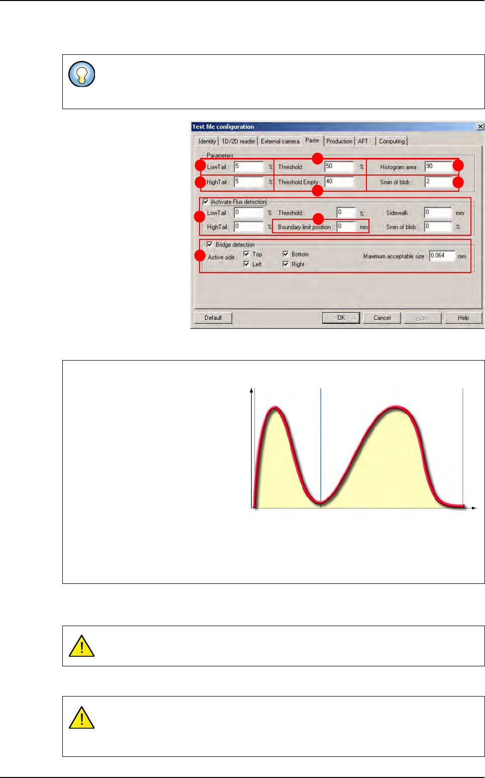
9.3.3 Processing parameters
.Low tail (A): background
noise eliminated on the
board (%).
High tail (B): background
noise eliminated on the
paste (%).
Threshold (C): distribution
between the board back-
ground and the solder (%).
Threshold empty
(
D
): con-
firmation of paste presence.
Histogram area (E): histo-
gram area relative to theo-
retical area (%) used for
threshold empty.
Smin of blob (F): minimum
size of the mask that the blob must consider. Theoretical surface area of the solder paste (%).
Tick Activate Flux detection (G) tick box to set Flux detection parameters. These parameters
are the same that for solder paste surface detection.
Boundary limit position (H): size limit of the flux.
The parameters of the Test file configuration window are those used, by default, for all
paste pads. These parameters are, however, individually adjustable for each paste pad
in Pad edition.
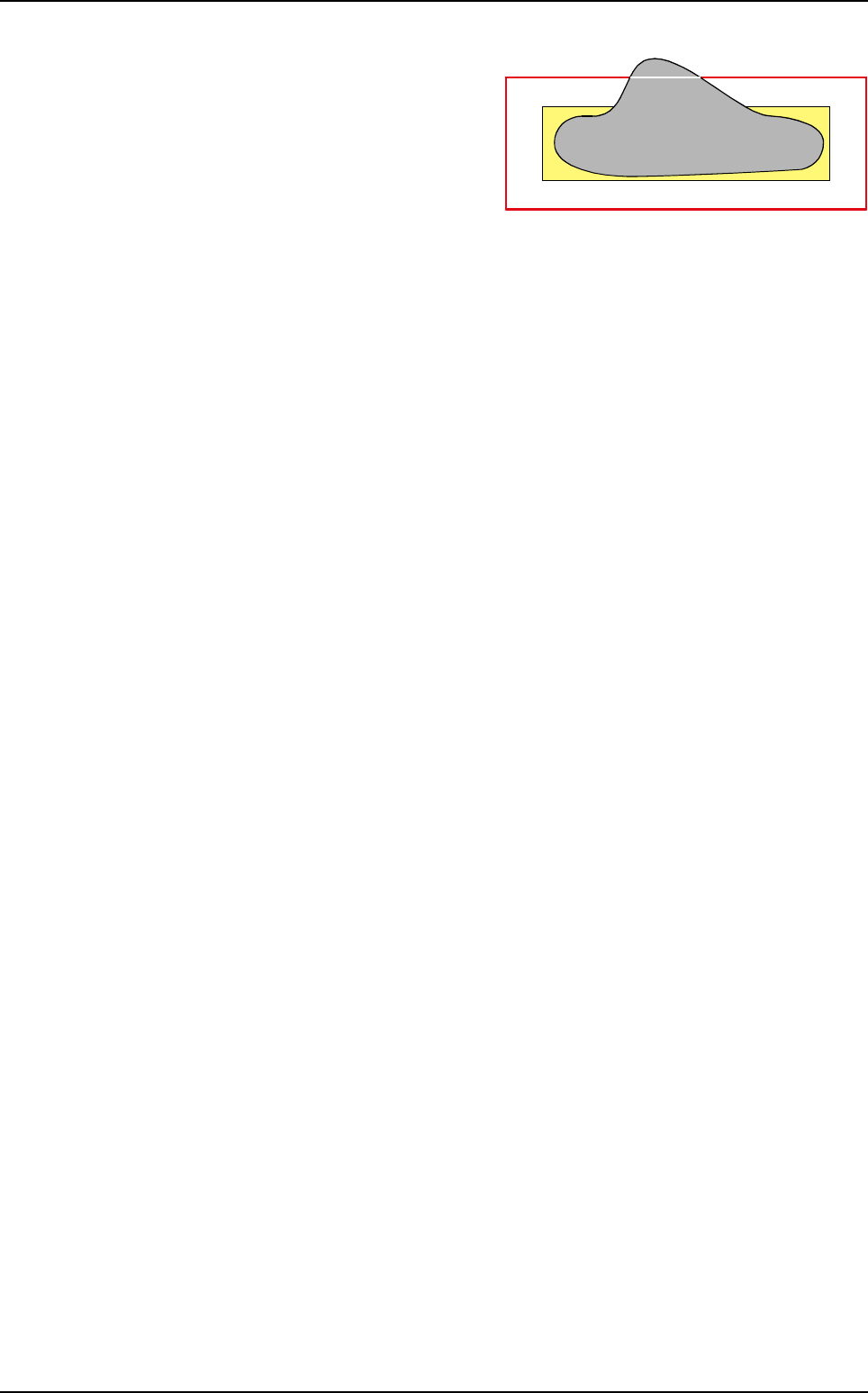
The blob’s first step is to generate a histogram on its search area.
Low tail: percentage of the total
number of pixels to be ignored in the
threshold calculation. These pixels
are removed from the bottom of the
histogram.
High tail
: percentage of the total num-
ber of pixels to be ignored in the
threshold calculation. These pixels are
removed from the top of the histogram.
Threshold: all the pixels in the blob’s
search area found above this thresh-
old are considered to be solder paste. This threshold is a percentage of maximum gray level.
Empty threshold: if the average of the histogram’s gray levels is below this threshold, this
means that there is no paste.
If you do not tick this box the
Flux detection parameters
are not taken into account.
If we detect a white shape whose sides stick out the pad size + 15 %, we do not take
care of this shape.
This value must be included between - 50 % to 100 %.
A
B
C
D
E
F
G
H
I
0 255Gray levels
L
ow
tail
Hi
g
h
tail
N
u
m
b
e
r
o
f
p
i
x
e
l
s
Th
res
h
o
ld
Background
Paste
Solder paste inspection
2D solder paste inspection
Vision 2007 4.10 User Manual Rev 01 9 - 7
Bridge detection ( I ): the short circuit detec-
tion feature can be activated by picking the op-
tion Bridge detection.
The short circuit detection can be set for all pads
by using the Paste tab in the test file configu-
ration window, or by using the Edit pad screen
to set each pad individually (with this way, the
propagation, propagation by topology and prop-
agation by jedec are available).
For each case the following parameters should be set:
The side of the pad to activate.
The maximum size of the bridge length. (0.100 mm is the default value defined in the .ini file,
under [Paste] keyword).
Solder paste inspection
2D solder paste inspection
9 - 8 Vision 2007 4.10 User Manual Rev 01
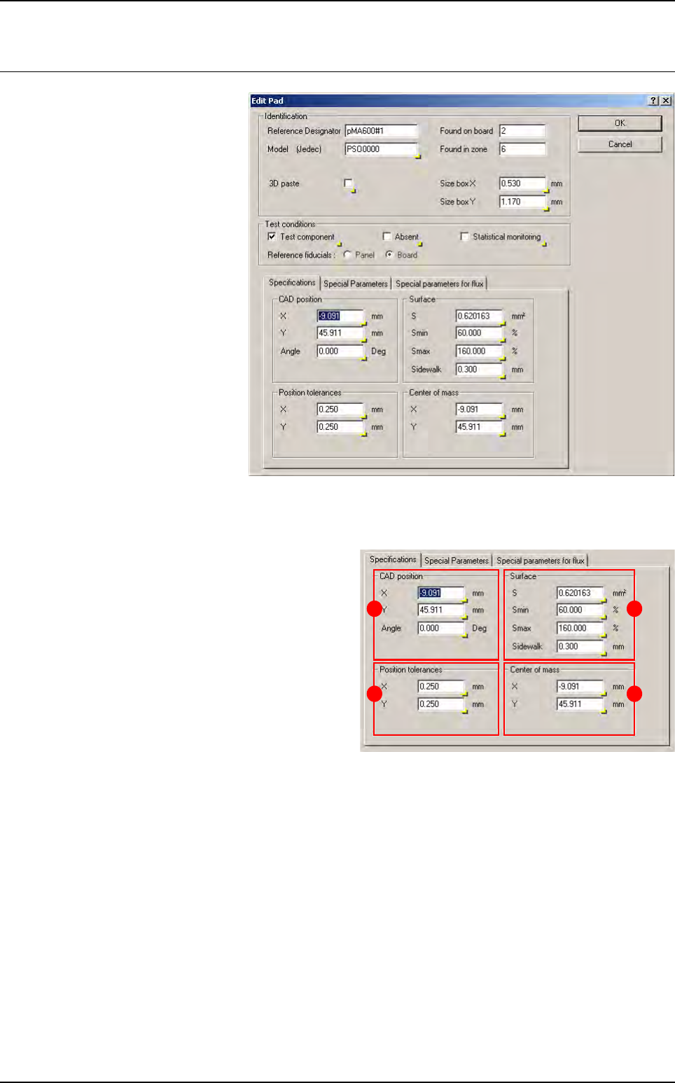
9.4 Paste pad edition
When you click on a paste pad
in the .tst file, the edition win-
dow below appears.
9.4.1 Specifications tab
In
CAD position
(
A
) section, enter the CAD
X and Y coordinates of the paste deposit.
In Position tolerances (B) section, enter
the acceptable tolerance of X and Y on the
position of the centre of gravity of the paste
deposit found (in 1/100th mm).
In Surface (C) section:
S
: theoretical surface area of paste deposit.
Smin & Smax: minimum and maximum ac-
ceptable surface area of paste.
Sidewalk: blob search area = theoretical
paste deposit area + sidewalk.
In Center of mass (D) section, enter the X and Y coordinates of center of gravity.
A
B
C
D