VI User Manual.pdf - 第291页
2D solder paste inspection Vision 2007 4.10 User Manua l Rev 01 9 - 13 9.7 Solder paste inspection results 9.7.1 Image in direct amber lighting (level 1) Characteristics of this lighting: Panel + track : uniform gra y …
2D solder paste inspection
9 - 12 Vision 2007 4.10 User Manual Rev 01
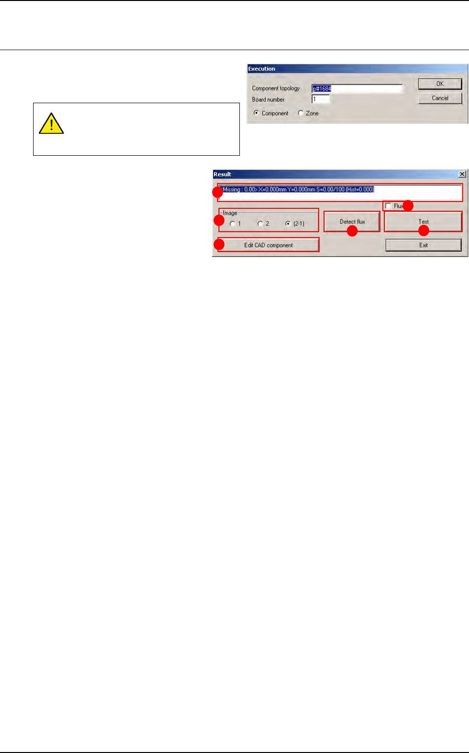
9.6 Paste pad execution (Ctrl + E)
The paste pad test is run as for normal
components. You can perform the same tests by
topology, JEDEC, zone, etc.
In Image (A) section select the lighting
level to display in the image window:
1 Lighting level 1 (amber direct).
2 Lighting level 2 (blue peripheral).
2 - 1 Subtraction of the 2 images.
Press Edit CAD component (B) button
to edit the paste pad and change certain
parameters.
The field (C) displays test results (∆x, ∆y, %S: theoretical surface area of the pad, histogram result).
The Flux (D) tick box enable or disable the flux algorithm during the solder paste control.
Press Detect flux (E) button to run the flux detection on the level 1. Shapes found are displayed in the
Cognex console and their position and surface are shown in the result window of the Ctrl + E box.
Press Test (F) button to re-test the paste pad.
Display of the paste pad must be acti-
vated in the .tst file for the paste inspec-
tion to be possible.
A
B
C
D
F
E
2D solder paste inspection
Vision 2007 4.10 User Manual Rev 01 9 - 13
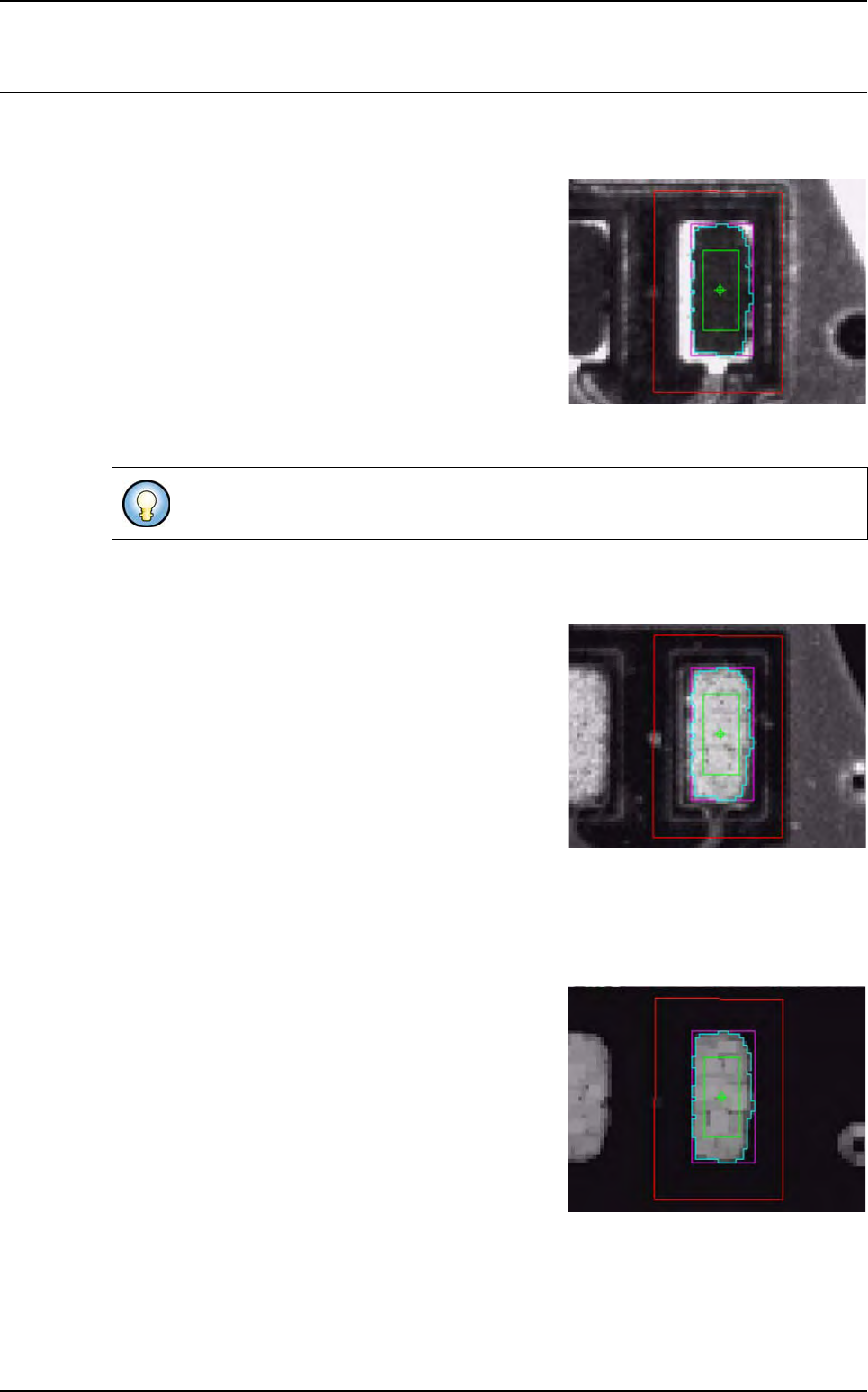
9.7 Solder paste inspection results
9.7.1 Image in direct amber lighting (level 1)
Characteristics of this lighting:
Panel + track: uniform gray
Reception pad: white
Paste: uniform black
Light level setting: intensity
60 axial amber
1 axial green
1 peripheral amber
1 peripheral blue
9.7.2 Image in peripheral blue lighting (level 2)
Characteristics of this lighting:
Panel: gray
Reception pad: uniform black
Paste: white
Light level setting: intensity
1 axial amber
1 axial green
1 peripheral amber
255 peripheral blue
9.7.3 Final image (image subtraction)
The result of the subtraction should be:
Panel + reception pad: black
Paste: white
Adjust intensity to obtain a smooth paste texture.
2D solder paste inspection
9 - 14 Vision 2007 4.10 User Manual Rev 01
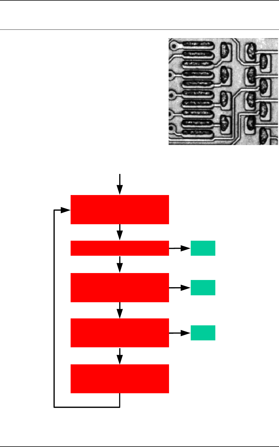
9.8 Solder paste with flux algorithm
The flux is a chemical product, part of the solder paste.
Under a direct lighting, flux becomes shiny when the
paste should be dark for our control.
As you can see in this image, there is lot of white shapes
in the paste due to the flux. This product cause many
dummy faults during our paste surface inspection.
The goal of this paste algorithm improvement is to delete
white shape from the picture so the normal algorithm
could return the reel paste surface.
9.8.1 Flux algorithm principle
Yes
End
No
End
No
Yes
End
No
Yes
Level 1 (direct lighting)
and Level 2 (horizontal lighting)
New level 1 (direct lighting)
and Level 2 (horizontal lighting)
We put all pixels of these blobs
to a dark value (cf ini file)
and save image
Is it a good paste pad ?
Is there any white blobs
into the paste pad
direct light image?
Is there any white blobs
completely included
in the paste pad?
Paste pad test
with the normal paste
algorithm