A10011-ASM-T53-EN-Spec-TX-micron-DMS - 第23页
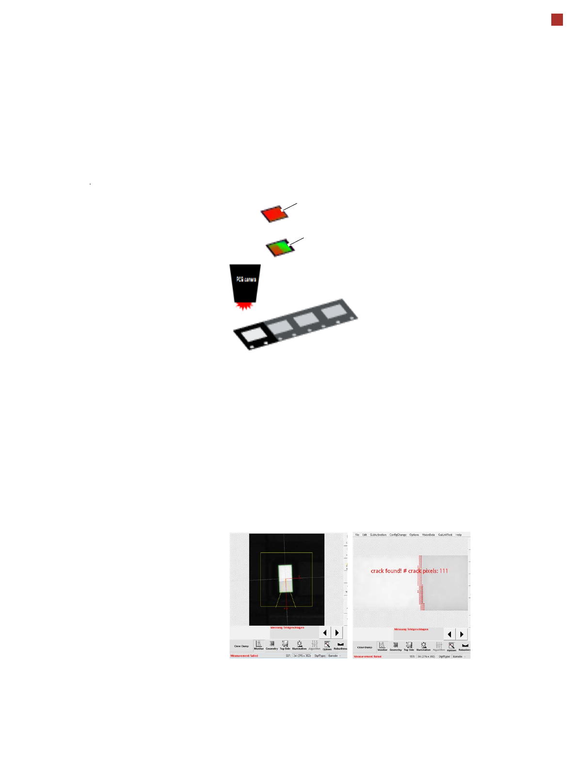
23 SIPLACE Vision Cracked Die and Chipping Inspection Crack Die Detection The cracked die inspection can detect breaks befo re removal from the tape, if the crack runs between tw o outer edge s of the die. Inspection is …
22
SIPLACE Vision
OnBoard Inspection and Pattern Matching
OnBoard Inspection
The OnBoard PCB Inspec-
tion (SW option) uses the
PCB camera to inspect criti-
cal areas of the board, spec-
ified by the user, e.g. under
BGA or shields just before or
after placement, to make
sure that all components
were placed or to make sure
that there are no objects in
the way of the placement
process.
It is also possible to inspect
the solder paste to make
sure that it is present. How-
ever, this must always be
performed at the first place-
ment machine, before place-
ment begins.
A requirement for all inspec-
tion tasks is that a "good pat-
tern" has been saved before
starting.
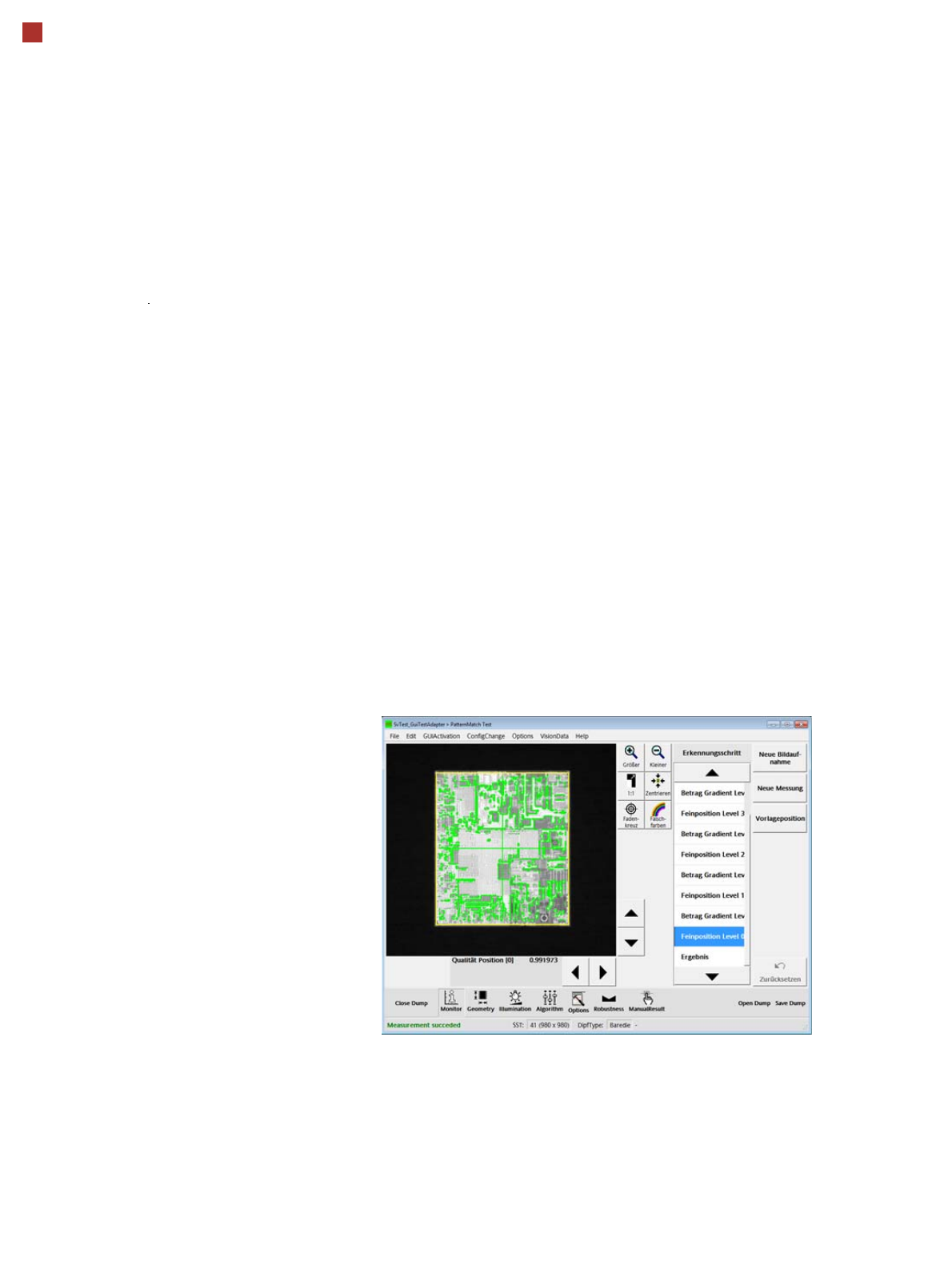
Pattern Matching
Pattern matching can be
used for components with
very fine contact pads, which
can not be detected with the
existing component camera
resolution. Searching and
detection is performed over a
larger area, which contains
unique structures (patterns).
Once the specified area has
been detected, the compo-
nent is aligned and placed
according to the position of
this area and in relation to the
substrate.
23
SIPLACE Vision
Cracked Die and Chipping Inspection
Crack Die Detection
The cracked die inspection
can detect breaks before
removal from the tape, if the
crack runs between two
outer edges of the die.
Inspection is performed
with the PCB camera. A
prerequisite for detection is
that the two parts of the die
are slightly inclined towards
one another. Detection is
possible via the differing
reflection angles of the two
surfaces which are inclined
towards one another.
Chipping Detection
Chipping detection allows
you to recognize chipped
areas on semiconductor
components.
Good
Bad

24
SIPLACE Vision
PCB position recognition
Fiducial criteria
Fiducial criteria
Locate 2 fiducials
Locate 3 fiducials
X-/Y-position, rotation angle, mean PCB distortion
Additional: shearing, distortion separately in X and Y direc-
tion
Fiducial shapes Synthetic fiducials: circle, cross, square, rectangle, dia-
mond, circular, square and rectangular contours, double
cross, pattern: any
Dimensions of patterns
Min. size
Max. size
0.5 mm
3 mm
Fiducial environment Clearance around reference fiducial not necessary if there
is no similar fiducial structure in the search area
Dimensions of synthetic fiducials
Min. X/Y size for circle
a
and rectangle 0.25 mm
Min. X/Y size for annulus and rectangle 0.3 mm
Min. X/Y size for cross 0.3 mm
Min. X/Y size for double cross 0.5 mm
Min. X/Y size for diamond 0.35 mm
Min. frame width for annulus and rectangle 0.1 mm
Min. bar width / bar distance for cross, double-cross 0.1 mm
Max. X/Y size for all fiducial shapes 3 mm
Max. bar width for cross/double-cross 1.5 mm
Minimum tolerances generally 2% of nominal dimension
Max. tolerances generally 20% of nominal dimension
a) To ensure high production quality of printed circuit boards, a minimum x/y size of 0.075 mm is permitted
for circular fiducials under the following conditions:
There are no other objects with a size of + 0.2 mm which are visible in the rectangular fiducial search
area. Example: Circular fiducials with an x/y size of 0.075 mm need a search area without visible objects
of: 0.075 mm + 0.2 mm = 0.275 mm.