西门子SIPLACE HS 60-设备参数_EN - 第22页
20 Vision Sensor Technology: PCB Vision Module Technical Data Reference marks Local marks Library memory Recognition of bad boards up to 3 (subpanels and multiple panels) up to 2 per component (may be of different type) …
19
Component Supply:
SIPLACE External Set-Up Station (Option)
Technical Data
Operating system Windows NT 4.0
Set-up check Per bar code scanner
Component table change Time expanded: 2 min / table side
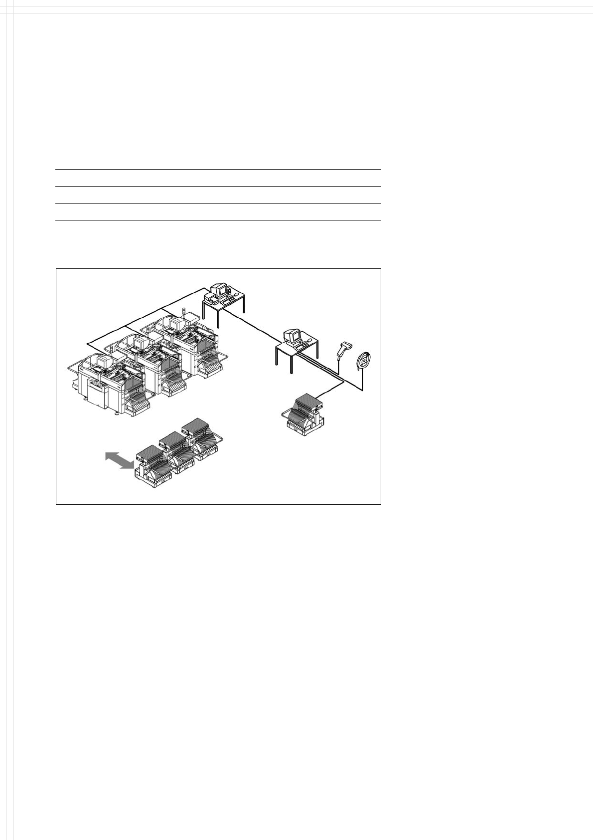
Description
The component changeover tables
can be set up and checked at an
external SIPLACE set-up station
quickly and without machine idle
time. The costs for production in-
volving a wide variety of compo-
nents are greatly reduced. During
the bar code check outside the
machine, 10 minutes of machine
standstill are eliminated per set-up
change. All current data from up to
4 lines are accessible over a link to
the line computer via a Local Area
Network (LAN).
Line
LAN
Line Computer
PC for External set-up
LAN Scanner
Additional changeover tables are
required for optimal use of the
set-up station.
Serial Interface
Tape Reel
with
Bar Code
Mobile
Changeover
Table
Mobile
Changeover
Tables
Example for SIPLACE Set-Up Station
20
Vision Sensor Technology:
PCB Vision Module
Technical Data
Reference marks
Local marks
Library memory
Recognition of bad boards
up to 3 (subpanels and multiple panels)
up to 2 per component
(may be of different type)
up to 255 types of reference marks
per subpanel
Image analysis Correlation principle (geometric
alignment) based on gray-scale values
Lighting method Front lighting
Recognition time fiducial/
bad board marks
0.4 s
Camera’s field of view 5.7 x 5.7 mm
Description
The SIPLACE HS-60 has a number
of vision modules and a central vi-
sion system to evaluate the re-
corded image data ensuring high
placement accuracy.
At the machine´s X-gantry the PCB
vision module is mounted. It is
used to find the PCBs´ positioning-
offsets within the conveyor sys-
tem.
This vision module is also required
to measure the machine origin
and/or the feeder positions on one
side of the table. It consists of a
single CCD camera with integrated
lighting and optics.
The offsets in the position of the
PCBs are determined with the
help of at least two but generally
three reference fiducial marks on
the PCB. When the PCB arrives at
the placement area the positioning
system with its PCB vision module
moves to the programmed mark
position.
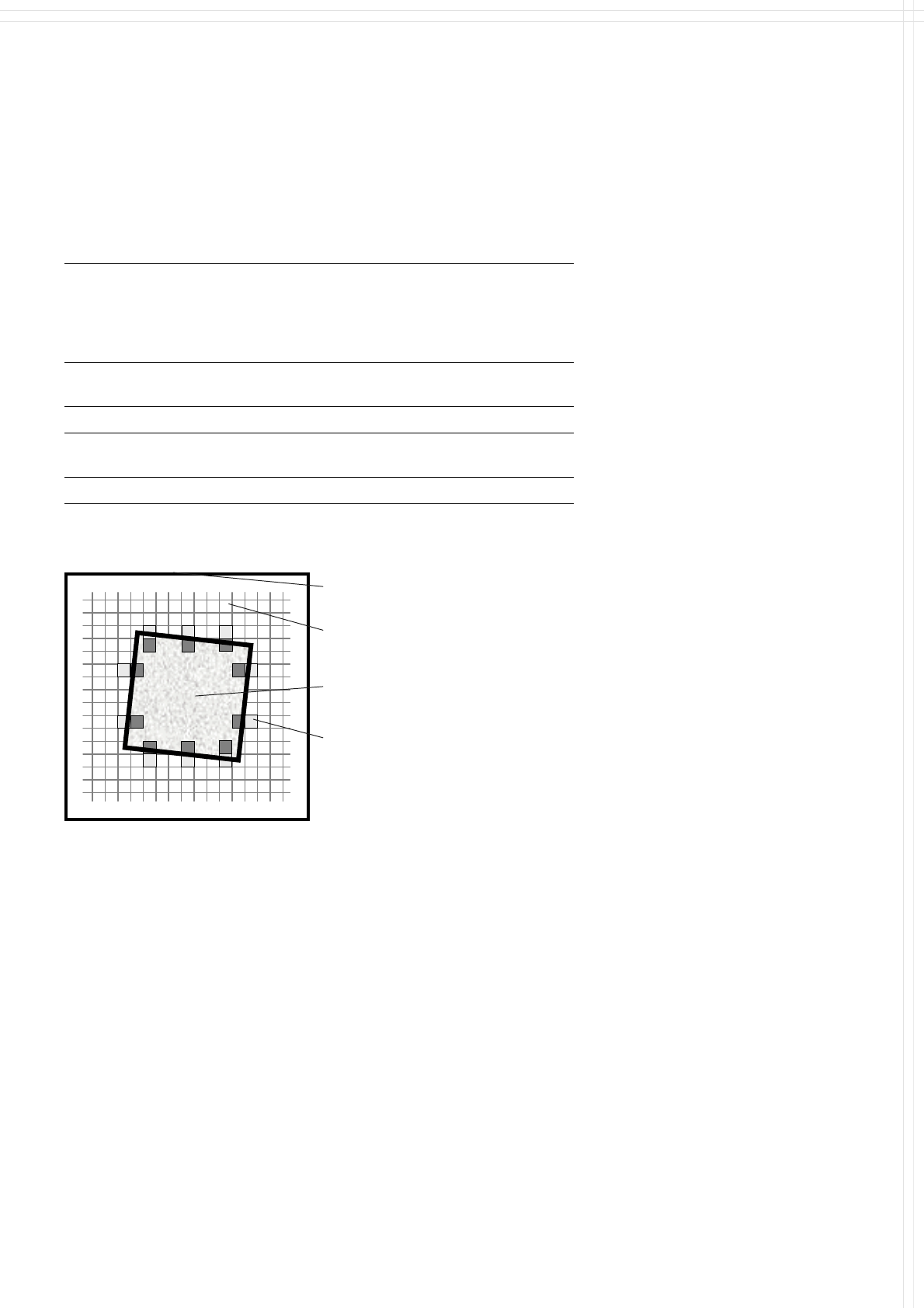
Using the Geometrical Alignment
allows to choose predefined
marks from a menu (e.g. cross,
circle, square). The size of the
mark is programmed at the Station
Computer. From this time on form
and size of the mark is defined and
known.
With this data the PCB vision
module is able to search and rec-
ognize the mark at the predefined
position on the PCB or ceramic
substrate without further assis-
tance. For this reason it places
several small evaluation windows
at the assumed border of the
mark. Within these evaluation win-
dows the vision system looks for
contrast transitions between
bright and dark. After finding such
contrasts the actual position of the
mark can be assigned by compari-
sion with the predefined – and
thus known – form and size.
Camera’s field of view
Pixel
Ink spot, e.g. square
Evaluation operations calculate
possible PCB offsets against given
values of X-, Y- and Theta-axis.
Saving the mark by teaching is not
necessary any more.
Additional functions of the PCB
vision module are recognition of
the position of the feeders and
ceramic substrate (optional) and
recording of the machine data in-
cluding mapping.
Geometrical Alignment
Evaluation window
In addition, the bad board recogni-
tion unit handles “ink spots” with
the aid of the PCB vision module.
21
Vision Sensor Technology:
PCB Position Recognition
Reference Mark Criteria
Locate 2 marks
Locate 3 marks in addition
X-/Y-position, rotation angle, mean distortion
Shear, distortion in X- and Y-direction
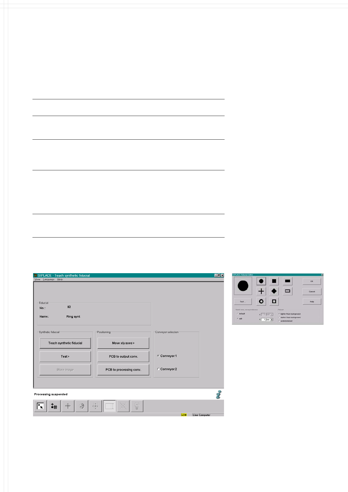
Mark shapes Synthetic marks e.g., circle, cross, square,
rectangle, rhombus, circular ring, square
ring, octagonal ring (choose from menu)
Mark surface:
Copper
Tin
Without oxidation and solder resist
Warp ≤ 1/10 of structure width,
both with good contrast to environment
Mark dimensions
Circle
Cross
Rectangle/square
Rhombus
Diameter: 0.3 - 3 mm
Length and width: 0.3 - 3 mm
Line thickness: 0.1 - 1.5 mm
Edge length: 0.3 - 3 mm
Transversal length: 0.3 - 3 mm
Mark environment Clearance around reference mark not
necessary if there is no similar mark
structure in the search area
Description
Different reference mark shapes
prove to be optimal depending on
the condition of the surface.
Particularly advisable for bare cop-
per surfaces with little oxidation is
the single cross. Maximum recog-
nition reliability is achieved due to
the high information content. Rec-
tangle, square and circle are less
“informative” but save space, are
rugged, and can even be used
when oxidation is at an advanced
stage.
Advisable for tinned structures are
circle or square because in this
case the ratio of the mark dimen-
sions to the presolder thickness is
particularly favorable.
Fiducial Editor
Teach Synthetic Fiducial