JANETS_INM.pdf - 第230页
JaNets In structio n Manual 7. Program Editor 7- 23 A rea Bad Mark W hen you sel ect “ Ed it ” or “ Browse ” in an “ Are a Bad M ark ” cell on t he “ Place ment Dat a ” scre en, the “ Area B ad Mark ” set tin g screen a …
JaNets Instruction Manual 7. Program Editor
7-22
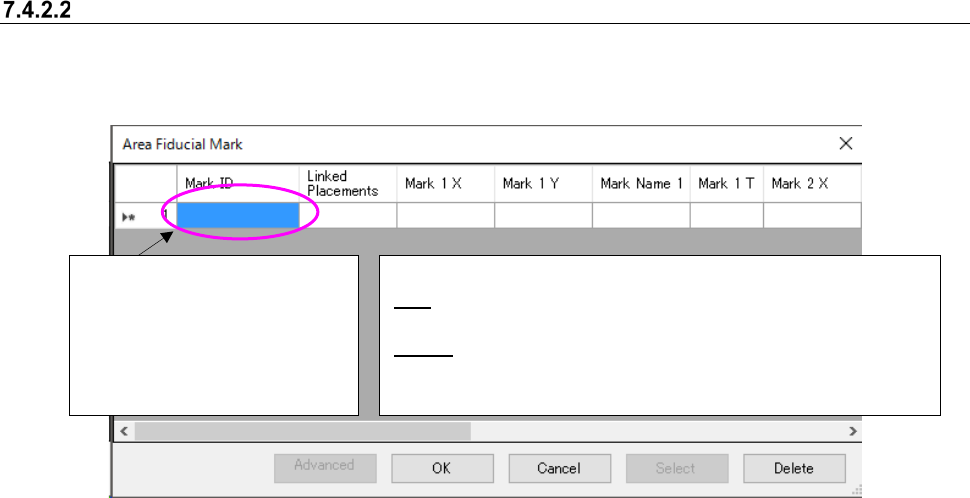
Area Fiducial Mark
When you select “Edit” or “Browse” in a “Mark” cell on the “Placement Data” screen, the “Area
Fiducial Mark” setting screen appears.
Figure 7.4-28 “Area Fiducial Mark” screen
Mark ID can be copied and pasted with the Ctrl+C key and the Ctrl+V key.
However, when the cell of mark ID is editing, the mark ID cannot be copied and pasted with the
Ctrl+C key and the Ctrl+V key.
[When a JX-350 and RS-1 are used]
If you finish creating one piece of mark data when you select “LED” as the “Mark Type,” the system
determines that Placement data has been completed.
<Operations of the buttons when “Edit” is selected>
OK: Goes back to the “Placement Data” screen, and saves the
input data. “NO” is displayed in the “Mark” cell.
Select: Goes back to the “Placement Data” screen, and displays
the selected mark ID in the “Mark” cell.
<Operations of the buttons when “Browse” is selected>
The mark ID is displayed in the
format “Mxxxx”
(up to eight characters).
The format “Sxxxx” (up to eight
characters): when Mark Type
is ”Solder” or “Solder (PWB)”.
JaNets Instruction Manual 7. Program Editor
7-23
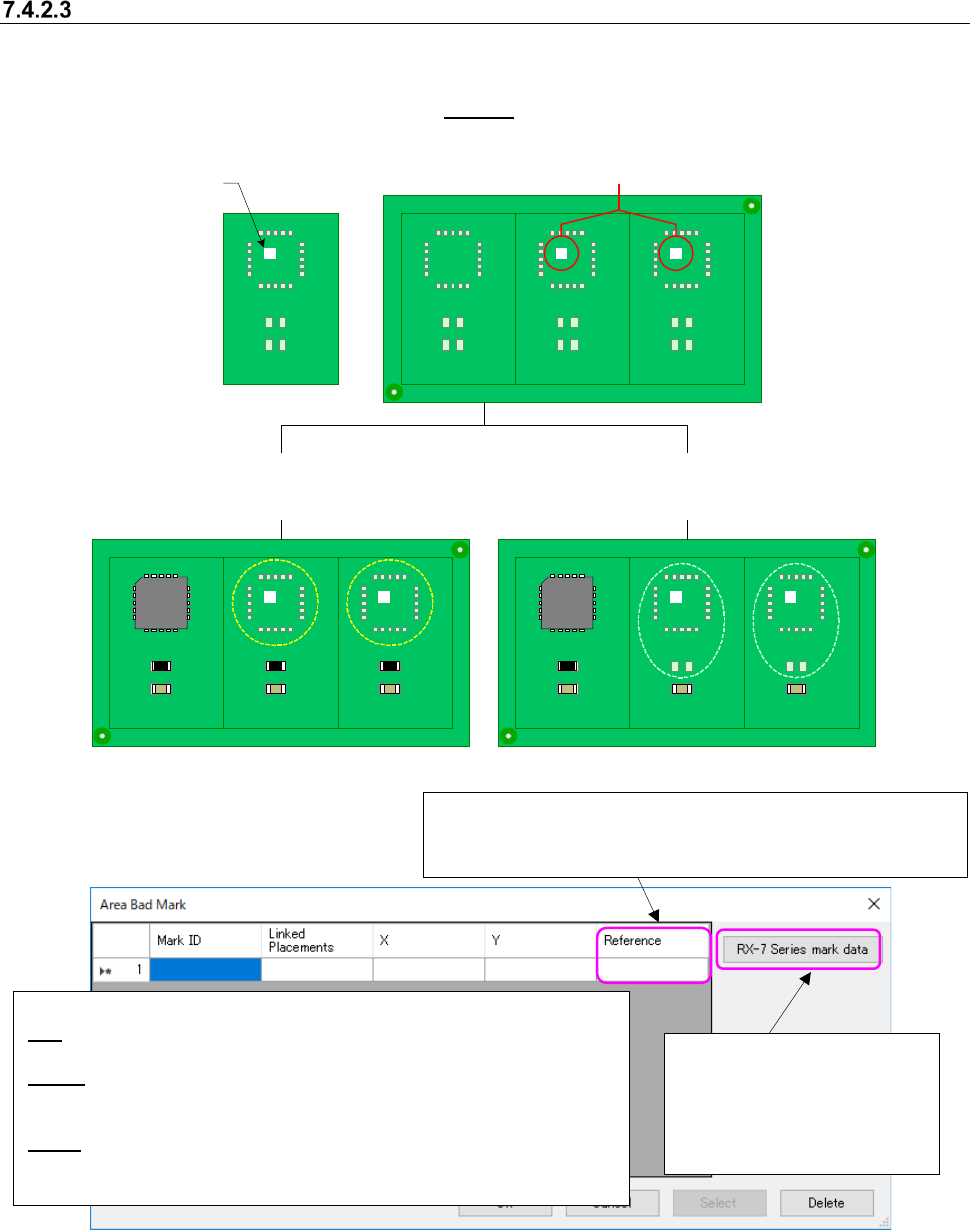
Area Bad Mark
When you select “Edit” or “Browse” in an “Area Bad Mark” cell on the “Placement Data” screen,
the “Area Bad Mark” setting screen appears. You can set up to 10,000 bad marks for each com-
ponent placement positions. See
Section “7.4.2.2 Area Fiducial Mark” for how to set data.
U1
U1
U1
U1
U1
U1
U1
R10
U1
U1
U1
C10
R10
C10
R10
C10
R10
C10
R10
C10
R10
C10
R10
C10
R10
C10
R10
C10
R10
C10
Circuit
Circuit
Circuit
Circuit
Circuit
Circuit
Circuit
Circuit
Circuit
Circuit
Figure 7.4-29 Image for setting an area bad mark
Figure 7.4-30 “Area Bad Mark” screen
Mark ID can be copied and pasted with the Ctrl+C key and the Ctrl+V key.
However, when the cell of mark ID is editing, the mark ID cannot be copied and pasted with the
Ctrl+C key and the Ctrl+V key.
Bad mark ID
BM001
Bad marks exist on a board.
When the bad mark ID “BM001” is assigned
to a component placement position “U1”
When the bad mark ID “BM001” is assigned to
component placement positions “U1” and “R10”
<Operations of buttons when you select “Edit”>
OK: Goes back to the “Placement Data” screen, and saves the input data. “NO”
appears in the “Mark” cell.
Select: Goes back to the “Placement Data” screen, and the selected mark ID is
displayed in the “Mark” cell.
<Operations of buttons when you select “Browse”>: The <OK> button is disabled.
Delete: Deletes bad mark data, changes all “Area Bad Mark” settings of Placement
data that use the selected bad mark ID to “NO” and goes back to the “Placement
Data” screen.
Reference: Sets the reference position of coordinates. When
you click the right button of a mouse, you can select one of the
followings: “Reference Circuit,” and “Circuit Origin.”
Sets bad mark information for
an RX-7 series.
See Section 7.4.1.3.1 “RX-7
series bad mark information”
for the detailed settings.
JaNets Instruction Manual 7. Program Editor
7-24
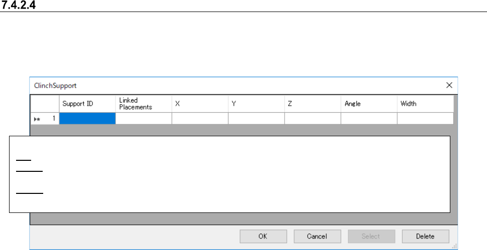
Clinch/ Clinch Support
If [Clinch] of Mounting Data Screen is [Clinch No. 1 ~ 4], perform the setting pattern which was set
by the clinch of component data is performed against the component at mounting point.
In case of [Edit] or [Ref.], Clinch Support Setting Screen is displayed.
Figure 7.4-31 “Clinch Support” screen
<Operations of buttons when you select “Edit”>
OK: Goes back to the “Placement Data” screen, and saves the input data. “NO” appears in the “Clinch” cell.
Select: Goes back to the “Placement Data” screen, and the selected mark ID is displayed in the “Clinch” cell.
<Operations of buttons when you select “Browse”>: The <OK> button is disabled.
Delete: Delete the Support Data.
Deletion is unable when the data using Support ID is existed.