IPC-CM-770D-1996 - 第103页
January 1996 IPC-CM-770 Part Five Assembly Processing Techniques 20.0 COMPONENT MOUNTING This Section is a general introduction to Sections 21 through 24, providing general process information. 20.1 General Consideration…
IPC-CM-770
Januaty
1996
conventional processes. Graphite can be used where ther-
mal conductivity per unit of weight is important.
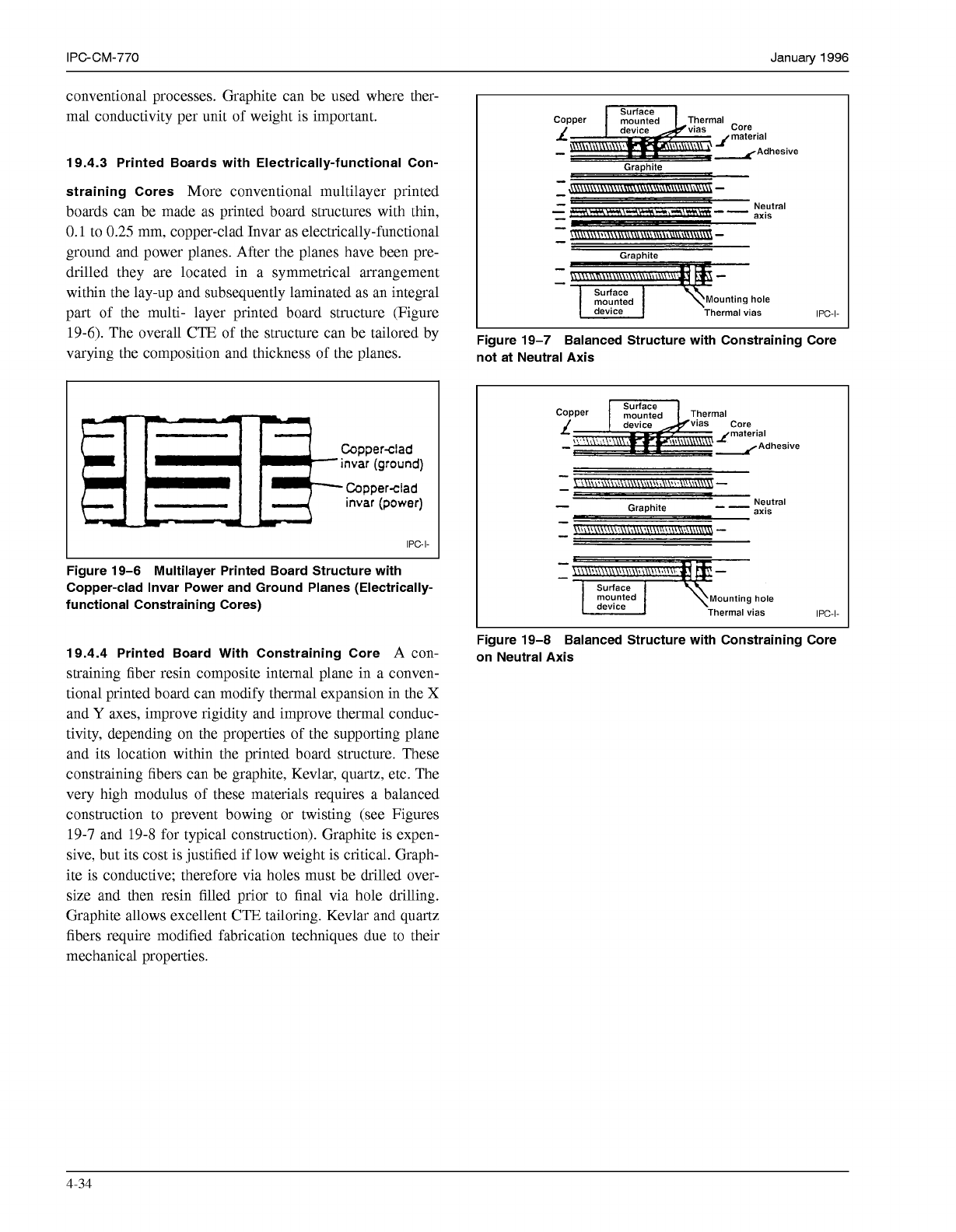
19.4.3 Printed Boards with Electrically-functional Con-
straining Cores
More conventional multilayer printed
boards can be made as printed board structures with thin,
0.1
to
0.25
mm, copper-clad Invar as electrically-functional
ground and power planes. After the planes have been pre-
drilled they are located in a symmetrical arrangement
within the lay-up and subsequently laminated as an integral
part of the multi- layer printed board structure (Figure
19-6).
The overall CTE of the structure can be tailored by
varying the composition and thickness of the planes.
IPC-I-
Figure 19-6 Multilayer Printed Board Structure with
Copper-clad Invar Power and Ground Planes (Electrically-
functional Constraining Cores)
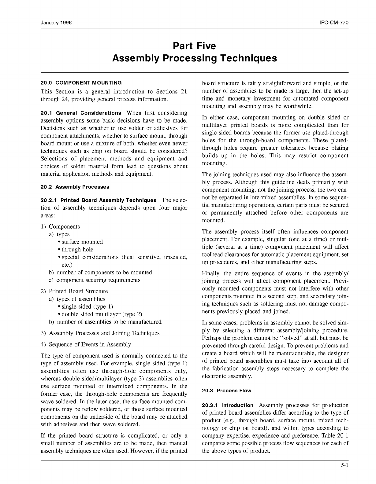
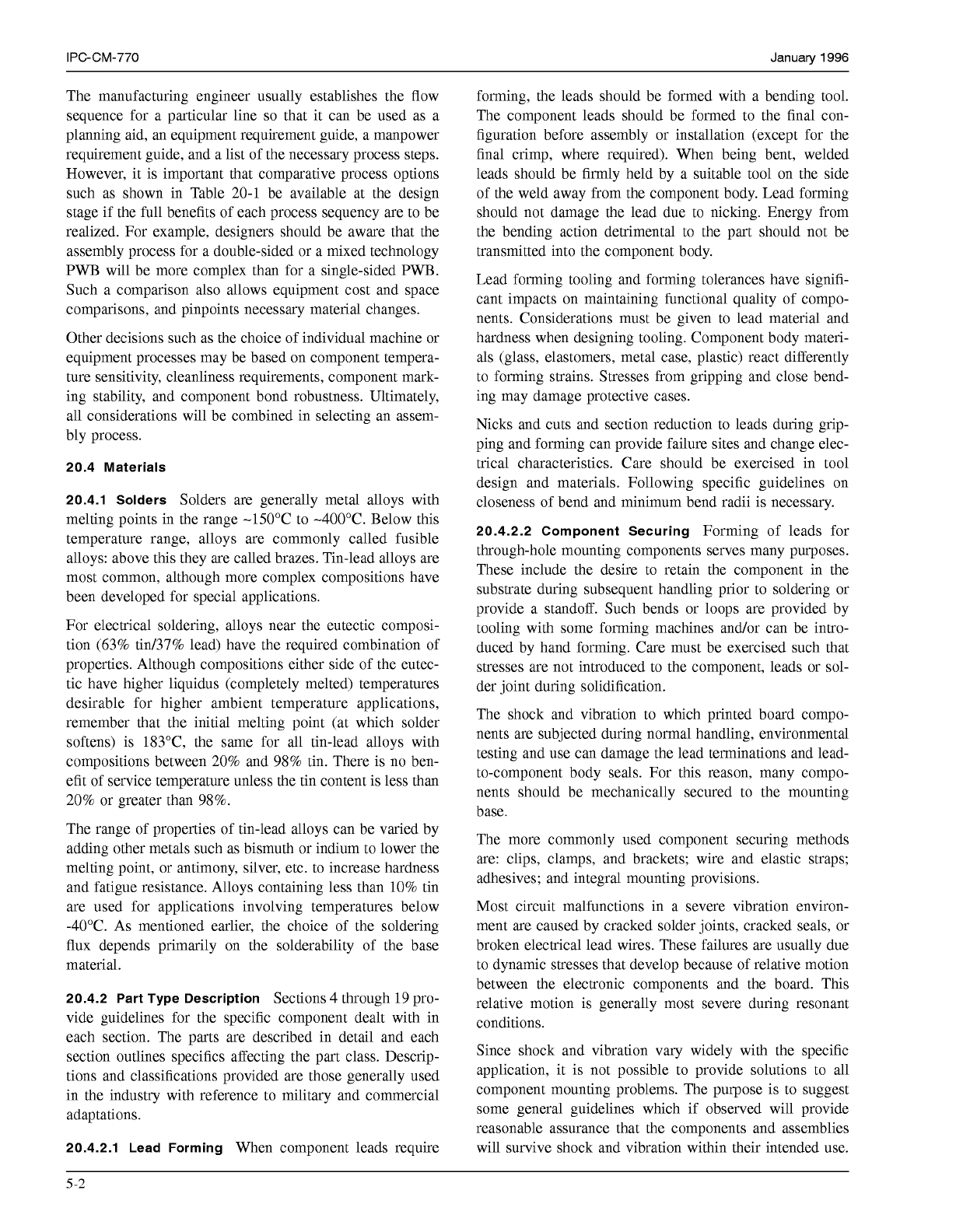
19.4.4 Printed Board With Constraining Core
A con-
straining fiber resin composite internal plane in a conven-
tional printed board can modify thermal expansion in the
X
and
Y
axes, improve rigidity and improve thermal conduc-
tivity, depending on the properties of the supporting plane
and its location within the printed board structure. These
constraining fibers can be graphite, Kevlar, quartz, etc. The
very high modulus of these materials requires a balanced
construction to prevent bowing or twisting (see Figures
19-7
and
19-8
for typical construction). Graphite is expen-
sive, but its cost is justified if low weight is critical. Graph-
ite is conductive; therefore via holes must be drilled over-
size and then resin filled prior to final via hole drilling.
Graphite allows excellent CTE tailoring. Kevlar and quartz
fibers require modified fabrication techniques due to their
mechanical properties.
e
Graphite
-
I
",",Ed
1
\Mounting hole
Thermal vias
IPC-I-
Figure 19-7 Balanced Structure with Constraining Core
not at Neutral Axis
L
material
-
-Adhesive
giz:d \Mounting hole
Thermal vias
IPC-I-
Figure 19-8 Balanced Structure with Constraining Core
on Neutral Axis
4-34
COPYRIGHT Association Connecting Electronics Industries
Licensed by Information Handling Services
COPYRIGHT Association Connecting Electronics Industries
Licensed by Information Handling Services
January
1996
IPC-CM-770
Part Five
Assembly Processing Techniques
20.0 COMPONENT MOUNTING
This Section is a general introduction to Sections 21
through 24, providing general process information.
20.1 General Considerations
When first considering
assembly options some basic decisions have to be made.
Decisions such as whether to use solder or adhesives for
component attachments, whether to surface mount, through
board mount or use a mixture of both, whether even newer
techniques such as chip on board should be considered?
Selections of placement methods and equipment and
choices of solder material form lead to questions about
material application methods and equipment.
20.2 Assembly Processes
20.2.1 Printed Board Assembly Techniques
The selec-
tion of assembly techniques depends upon four major
areas:
1)
Components
4
types
surface mounted
through hole
special considerations (heat sensitive, unsealed,
etc.)
b) number of components to be mounted
c) component securing requirements
2) Printed Board Structure
a) types of assemblies
single sided (type
1)
double sided multilayer (type 2)
b) number of assemblies to be manufactured
3)
Assembly Processes and Joining Techniques
4) Sequence of Events in Assembly
The type of component used is normally connected to the
type of assembly used. For example, single sided (type
1)
assemblies often use through-hole components only,
whereas double sided/multilayer (type 2) assemblies often
use surface mounted or intermixed components. In the
former case, the through-hole components are frequently
wave soldered. In the later case, the surface mounted com-
ponents may be reflow soldered, or those surface mounted
components on the underside of the board may be attached
with adhesives and then wave soldered.
If the printed board structure is complicated, or only a
small number of assemblies are to be made, then manual
assembly techniques are often used. However, if the printed
board structure is fairly straightforward and simple, or the
number of assemblies to be made is large, then the set-up
time and monetary investment for automated component
mounting and assembly may be worthwhile.
In either case, component mounting on double sided or
multilayer printed boards is more complicated than for
single sided boards because the former use plated-through
holes for the through-board components. These plated-
through holes require greater tolerances because plating
builds up in the holes. This may restrict component
mounting.
The joining techniques used may also influence the assem-
bly process. Although this guideline deals primarily with
component mounting, not the joining process, the two can-
not be separated in intermixed assemblies. In some sequen-
tial manufacturing operations, certain parts must be secured
or permanently attached before other components are
mounted.
The assembly process itself often influences component
placement. For example, singular (one at a time) or mul-
tiple (several at a time) component placement will affect
toolhead clearances for automatic placement equipment, set
up procedures, and other manufacturing steps.
Finally, the entire sequence of events in the assembly/
joining process will affect component placement. Previ-
ously mounted components must not interfere with other
components mounted in a second step, and secondary join-
ing techniques such as soldering must not damage compo-
nents previously placed and joined.
In some cases, problems in assembly cannot be solved sim-
ply by selecting a different assembly/joining procedure.
Perhaps the problem cannot be "solved" at all, but must be
prevented through careful design. To prevent problems and
create a board which will be manufacturable, the designer
of printed board assemblies must take into account all of
the fabrication assembly steps necessary to complete the
electronic assembly.
20.3 Process
Flow
20.3.1 Introduction
Assembly processes for production
of printed board assemblies differ according to the type of
product (e.g., through board, surface mount, mixed tech-
nology or chip on board), and within types according to
company expertise, experience and preference. Table 20-1
compares some possible process flow sequences for each of
the above types of product.
5-1
COPYRIGHT Association Connecting Electronics Industries
Licensed by Information Handling Services
COPYRIGHT Association Connecting Electronics Industries
Licensed by Information Handling Services
IPC-CM-770
Januaty
1996
The manufacturing engineer usually establishes the flow
sequence for a particular line
so
that it can be used as a
planning aid, an equipment requirement guide, a manpower
requirement guide, and a list of the necessary process steps.
However, it is important that comparative process options
such as shown in Table
20-1
be available at the design
stage if the full benefits of each process sequency are to be
realized. For example, designers should be aware that the
assembly process for a double-sided or a mixed technology
PWB
will be more complex than for a single-sided
PWB.
Such a comparison also allows equipment cost and space
comparisons, and pinpoints necessary material changes.
Other decisions such as the choice of individual machine or
equipment processes may be based on component tempera-
ture sensitivity, cleanliness requirements, component mark-
ing stability, and component bond robustness. Ultimately,
all considerations will be combined in selecting an assem-
bly process.
20.4 Materials
20.4.1 Solders
Solders are generally metal alloys with
melting points in the range -150°C to -400°C. Below this
temperature range, alloys are commonly called fusible
alloys: above this they are called brazes. Tin-lead alloys are
most common, although more complex compositions have
been developed for special applications.
For electrical soldering, alloys near the eutectic composi-
tion (63% tin/37% lead) have the required combination of
properties. Although compositions either side of the eutec-
tic have higher liquidus (completely melted) temperatures
desirable for higher ambient temperature applications,
remember that the initial melting point (at which solder
softens) is 183"C, the same for all tin-lead alloys with
compositions between
20%
and
98%
tin. There is no ben-
efit of service temperature unless the tin content is less than
20%
or greater than
98%.
The range of properties of tin-lead alloys can be varied by
adding other metals such as bismuth or indium to lower the
melting point, or antimony, silver, etc. to increase hardness
and fatigue resistance. Alloys containing less than
10%
tin
are used for applications involving temperatures below
-40°C. As mentioned earlier, the choice of the soldering
flux depends primarily on the solderability of the base
material.
20.4.2 Part Type Description
Sections 4 through
19
pro-
vide guidelines for the specific component dealt with in
each section. The parts are described in detail and each
section outlines specifics affecting the part class. Descrip-
tions and classifications provided are those generally used
in the industry with reference to military and commercial
adaptations.
20.4.2.1 Lead Forming
When component leads require
forming, the leads should be formed with a bending tool.
The component leads should be formed to the final con-
figuration before assembly or installation (except for the
final crimp, where required). When being bent, welded
leads should be firmly held by a suitable tool on the side
of the weld away from the component body. Lead forming
should not damage the lead due to nicking. Energy from
the bending action detrimental to the part should not be
transmitted into the component body.
Lead forming tooling and forming tolerances have signifi-
cant impacts on maintaining functional quality of compo-
nents. Considerations must be given to lead material and
hardness when designing tooling. Component body materi-
als (glass, elastomers, metal case, plastic) react differently
to forming strains. Stresses from gripping and close bend-
ing may damage protective cases.
Nicks and cuts and section reduction to leads during grip-
ping and forming can provide failure sites and change elec-
trical characteristics. Care should be exercised in tool
design and materials. Following specific guidelines on
closeness of bend and minimum bend radii is necessary.
20.4.2.2 Component Securing
Forming of leads for
through-hole mounting components serves many purposes.
These include the desire to retain the component in the
substrate during subsequent handling prior to soldering or
provide a standoff. Such bends or loops are provided by
tooling with some forming machines and/or can be intro-
duced by hand forming. Care must be exercised such that
stresses are not introduced to the component, leads or sol-
der joint during solidification.
The shock and vibration to which printed board compo-
nents are subjected during normal handling, environmental
testing and use can damage the lead terminations and lead-
to-component body seals. For this reason, many compo-
nents should be mechanically secured to the mounting
base.
The more commonly used component securing methods
are: clips, clamps, and brackets; wire and elastic straps;
adhesives; and integral mounting provisions.
Most circuit malfunctions in a severe vibration environ-
ment are caused by cracked solder joints, cracked seals, or
broken electrical lead wires. These failures are usually due
to dynamic stresses that develop because of relative motion
between the electronic components and the board. This
relative motion is generally most severe during resonant
conditions.
Since shock and vibration vary widely with the specific
application, it is not possible to provide solutions to all
component mounting problems. The purpose is to suggest
some general guidelines which if observed will provide
reasonable assurance that the components and assemblies
will survive shock and vibration within their intended use.
5-2
COPYRIGHT Association Connecting Electronics Industries
Licensed by Information Handling Services
COPYRIGHT Association Connecting Electronics Industries
Licensed by Information Handling Services