IPC-CM-770D-1996 - 第105页
January 1996 IPC-CM-770 Table 20-1 Through Hole and Surface Mount Assembly Process Flow Comparison ~~ Surface Mount Single Sided A Surface Mount Single Sided B Surface Mount through Board Mi Surface Mount Double Sided PR…
IPC-CM-770
Januaty
1996
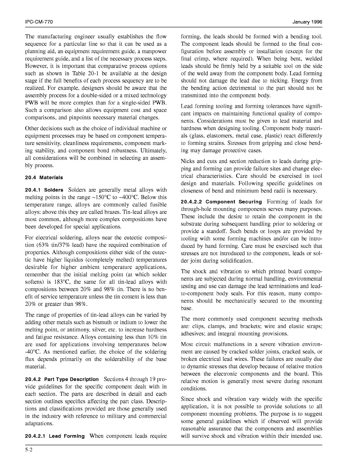
The manufacturing engineer usually establishes the flow
sequence for a particular line
so
that it can be used as a
planning aid, an equipment requirement guide, a manpower
requirement guide, and a list of the necessary process steps.
However, it is important that comparative process options
such as shown in Table
20-1
be available at the design
stage if the full benefits of each process sequency are to be
realized. For example, designers should be aware that the
assembly process for a double-sided or a mixed technology
PWB
will be more complex than for a single-sided
PWB.
Such a comparison also allows equipment cost and space
comparisons, and pinpoints necessary material changes.
Other decisions such as the choice of individual machine or
equipment processes may be based on component tempera-
ture sensitivity, cleanliness requirements, component mark-
ing stability, and component bond robustness. Ultimately,
all considerations will be combined in selecting an assem-
bly process.
20.4 Materials
20.4.1 Solders
Solders are generally metal alloys with
melting points in the range -150°C to -400°C. Below this
temperature range, alloys are commonly called fusible
alloys: above this they are called brazes. Tin-lead alloys are
most common, although more complex compositions have
been developed for special applications.
For electrical soldering, alloys near the eutectic composi-
tion (63% tin/37% lead) have the required combination of
properties. Although compositions either side of the eutec-
tic have higher liquidus (completely melted) temperatures
desirable for higher ambient temperature applications,
remember that the initial melting point (at which solder
softens) is 183"C, the same for all tin-lead alloys with
compositions between
20%
and
98%
tin. There is no ben-
efit of service temperature unless the tin content is less than
20%
or greater than
98%.
The range of properties of tin-lead alloys can be varied by
adding other metals such as bismuth or indium to lower the
melting point, or antimony, silver, etc. to increase hardness
and fatigue resistance. Alloys containing less than
10%
tin
are used for applications involving temperatures below
-40°C. As mentioned earlier, the choice of the soldering
flux depends primarily on the solderability of the base
material.
20.4.2 Part Type Description
Sections 4 through
19
pro-
vide guidelines for the specific component dealt with in
each section. The parts are described in detail and each
section outlines specifics affecting the part class. Descrip-
tions and classifications provided are those generally used
in the industry with reference to military and commercial
adaptations.
20.4.2.1 Lead Forming
When component leads require
forming, the leads should be formed with a bending tool.
The component leads should be formed to the final con-
figuration before assembly or installation (except for the
final crimp, where required). When being bent, welded
leads should be firmly held by a suitable tool on the side
of the weld away from the component body. Lead forming
should not damage the lead due to nicking. Energy from
the bending action detrimental to the part should not be
transmitted into the component body.
Lead forming tooling and forming tolerances have signifi-
cant impacts on maintaining functional quality of compo-
nents. Considerations must be given to lead material and
hardness when designing tooling. Component body materi-
als (glass, elastomers, metal case, plastic) react differently
to forming strains. Stresses from gripping and close bend-
ing may damage protective cases.
Nicks and cuts and section reduction to leads during grip-
ping and forming can provide failure sites and change elec-
trical characteristics. Care should be exercised in tool
design and materials. Following specific guidelines on
closeness of bend and minimum bend radii is necessary.
20.4.2.2 Component Securing
Forming of leads for
through-hole mounting components serves many purposes.
These include the desire to retain the component in the
substrate during subsequent handling prior to soldering or
provide a standoff. Such bends or loops are provided by
tooling with some forming machines and/or can be intro-
duced by hand forming. Care must be exercised such that
stresses are not introduced to the component, leads or sol-
der joint during solidification.
The shock and vibration to which printed board compo-
nents are subjected during normal handling, environmental
testing and use can damage the lead terminations and lead-
to-component body seals. For this reason, many compo-
nents should be mechanically secured to the mounting
base.
The more commonly used component securing methods
are: clips, clamps, and brackets; wire and elastic straps;
adhesives; and integral mounting provisions.
Most circuit malfunctions in a severe vibration environ-
ment are caused by cracked solder joints, cracked seals, or
broken electrical lead wires. These failures are usually due
to dynamic stresses that develop because of relative motion
between the electronic components and the board. This
relative motion is generally most severe during resonant
conditions.
Since shock and vibration vary widely with the specific
application, it is not possible to provide solutions to all
component mounting problems. The purpose is to suggest
some general guidelines which if observed will provide
reasonable assurance that the components and assemblies
will survive shock and vibration within their intended use.
5-2
COPYRIGHT Association Connecting Electronics Industries
Licensed by Information Handling Services
COPYRIGHT Association Connecting Electronics Industries
Licensed by Information Handling Services
January
1996
IPC-CM-770
Table 20-1 Through Hole and Surface Mount Assembly Process
Flow
Comparison
~~
Surface Mount
Single Sided
A
Surface
Mount
Single Sided B
Surface Mount
through Board
Mi
Surface Mount
Double Sided
PRECLEAN
Through
Board
n
PRECLEAN
W
PRECLEAN
u
PRECLEAN
PRECLEAN
APPLY SOLDER
I
CREAM
APPLY SOLDER
U
APPLY SOLDER
CREAM
APPLY COMP.
ADHESIVE
PICWPLACE
COMPONENTS
SIDE
1
ADHESIVE
SIDE
1
1
PlC"WUPTLOACE
I
COMPONENTS
I
PlC%$CE
I
COMPONENTS
COMPONENTS
AUTO INSERT
COMPONENTS
MANUAL INSERT
I
I
I
I
MANUAL
COMPONENTS
PICWPLACE
I
I
MANUAL
COMPONENTS
PICWPLACE
[Tl
CURE SOLDER
I
CRYM
I
CURE SOLDER
CURE SOLDER
CREAM
SOLDERCREAM
CLEAN
U
FLOW MELT
SOLDER CREAM SOLDERCREAM
FLOW MELT
I
AUTO PICK
6
SIDE
2
AUTO INSERT
COMPONENTS
ANUAL INSERT
COMPONENTS
PUCL1
MANUAL PICK
6
I
PREHEAT THEN
MACHINE
SOLDER
I
I
PREHEAT THEN
MACHINE
SOLDER
I
FLOW MELT
SOLDER CREAM
CLEAN
MACHINE
SOLDER
I
CLEAN
I
REPAIR
REPAIR
.
RETEST
REPAIR
RETEST
REPAIR
RETEST
REPAIR
RETEST
I
RETEST
5-3
COPYRIGHT Association Connecting Electronics Industries
Licensed by Information Handling Services
COPYRIGHT Association Connecting Electronics Industries
Licensed by Information Handling Services
IPC-CM-770
Januaty
1996
The extent to which the user wishes to implement these
guidelines may ultimately be validated by actual tests of
the assembled printed board in its intended shock and
vibration environment.
The ultimate ability of components to survive in shock and
vibration environments will depend upon the degree of
consideration given to the following factors:
The worst case levels of shock and vibration environment
for the entire structure in which the printed board assem-
bly resides and the ultimate level of this environment that
is actually transmitted to the components mounted on the
board. Particular attention should be given to equipment
which will be subjected to random vibration.
The method of mounting the board in the equipment to
reduce the effects of this environment, specifically the
number of board mounting supports and their interval and
complexity.
The attention given to the mechanical design of the
board; specifically its size, shape, type of material, mate-
rial thickness and degree of resistance to bowing and
flexing that the design provides.
The shape, mass, and location of the components
mounted on the board.
The component lead wire strain relief design as provided
by its package, lead spacing, lead bending, or a combina-
tion of these plus the addition of restraining devices.
The attention paid to workmanship during board assem-
bly
so
as to insure that component leads are properly
bent, not nicked and that components are installed in a
manner which minimizes component movement.
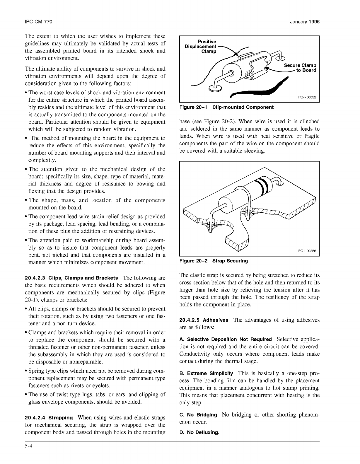
20.4.2.3 Clips, Clamps and Brackets
The following are
the basic requirements which should be adhered to when
components are mechanically secured by clips (Figure
20-l),
clamps or brackets:
All clips, clamps or brackets should be secured to prevent
their rotation, such as by using two fasteners or one fas-
tener and a non-turn device.
Clamps and brackets which require their removal in order
to replace the component should be secured with a
threaded fastener or other non-permanent fastener, unless
the subassembly in which they are used is considered to
be disposable or nonrepairable.
Spring type clips which need not be removed during com-
ponent replacement may be secured with permanent type
fasteners such as rivets or eyelets.
The use of twist type lugs, tabs, or ears, and clipping of
glass envelope components, should be avoided.
20.4.2.4 Strapping
When using wires and elastic straps
for mechanical securing, the strap is wrapped over the
component body and passed through holes in the mounting
Positive
re Clamp
to Board
IPC-I-O0032
Figure 20-1 Clip-mounted Component
base (see Figure
20-2).
When wire is used it is clinched
and soldered in the same manner as component leads to
lands. When wire is used with heat sensitive or fragile
components the part of the wire on the component should
be covered with a suitable sleeving.
Figure 20-2 Strap Securing
The elastic strap is secured by being stretched to reduce its
cross-section below that of the hole and then returned to its
larger than hole size by relieving the tension after it has
been passed through the hole. The resiliency of the strap
holds the component in place.
20.4.2.5 Adhesives
The advantages of using adhesives
are as follows:
A. Selective Deposition Not Required
Selective applica-
tion is not required and the entire circuit can be covered.
Conductivity only occurs where component leads make
contact during the thermal stage.
B. Extreme Simplicity
This is basically a one-step pro-
cess. The bonding film can be handled by the placement
equipment in a manner analogous to hot stamp printing.
This means that placement concurrent with heating is the
only step.
C. No Bridging
No
bridging or other shorting phenom-
enon occur.
D. No Defluxing.
5-4
COPYRIGHT Association Connecting Electronics Industries
Licensed by Information Handling Services
COPYRIGHT Association Connecting Electronics Industries
Licensed by Information Handling Services