IPC-CM-770D-1996 - 第121页
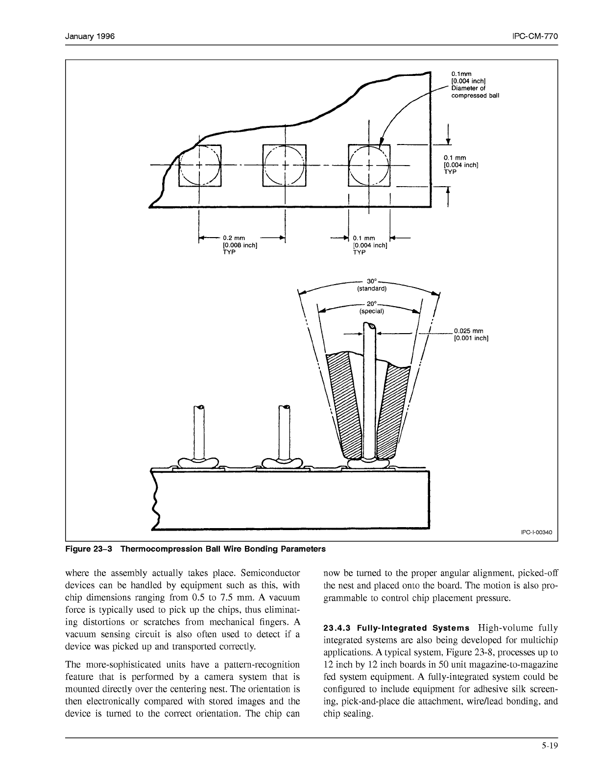
January 1996 IPC-CM-770 0.1 mm [0.004 inch] TYP TYP TYP ,0.025 mm [0.001 inch] ball IPC-1-00340 Figure 23-3 Thermocompression Ball Wire Bonding Parameters where the assembly actually takes place. Semiconductor now be tur…
IPC-CM-770
Januaty
1996
3.
Bond
Force
R
I
6.
Second Search
9.
Ball is
Reformed
Torch
1.
Home
Wire
of
Wire
Ball on End
n
4.
Tip Withdrawn
7.
Wedge Bonding
Operation
o1
,ce
8.
Alt. Tail
Pulling
!.
Search
i.
Work Moved Toward
Next
Position
B.
Tip
Withdrawn
m
Wedge
Diffusion
Bond
9.
Alt. Tail
Pulling
Ball
is
Retracted
d
IPC-1-00341
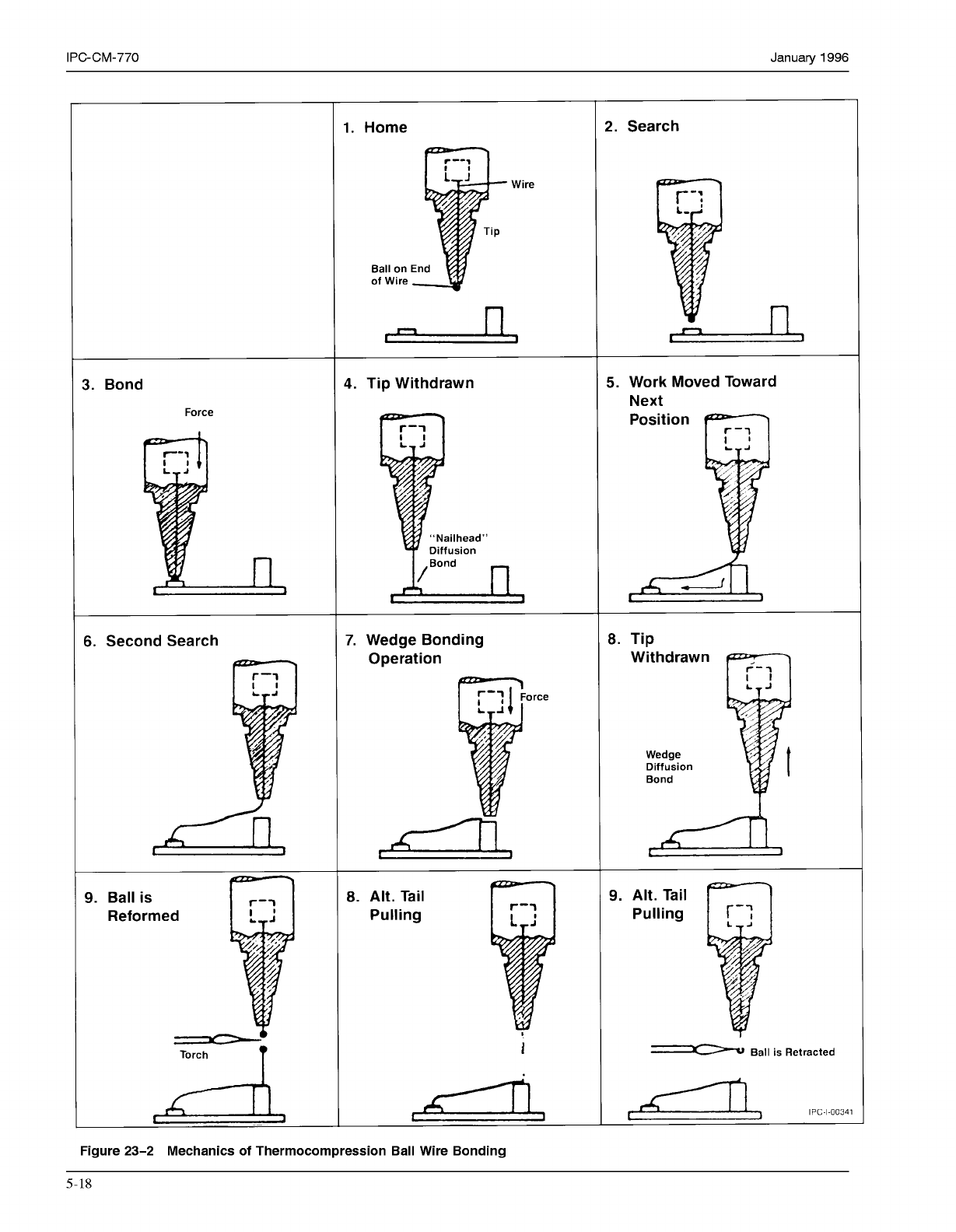
Figure
23-2
Mechanics
of
Thermocompression
Ball
Wire
Bonding
5-18
COPYRIGHT Association Connecting Electronics Industries
Licensed by Information Handling Services
COPYRIGHT Association Connecting Electronics Industries
Licensed by Information Handling Services
January
1996
IPC-CM-770
0.1
mm
[0.004
inch]
TYP
TYP TYP
,0.025
mm
[0.001
inch]
ball
IPC-1-00340
Figure 23-3 Thermocompression Ball Wire Bonding Parameters
where the assembly actually takes place. Semiconductor now be turned to the proper angular alignment, picked-off
devices can be handled by equipment such as this, with the nest and placed onto the board. The motion is also pro-
chip dimensions ranging from
0.5
to
7.5
mm.
A
vacuum grammable to control chip placement pressure.
force is typically used to pick up the chips, thus eliminat-
ing distortions or scratches from mechanical fingers.
A
vacuum sensing circuit is also often used to detect if a
23.4.3 Fully-Integrated Systems
High-volume fully
device was picked up and transported correctly.
integrated systems are also being developed for multichip
applications.
A
typical system, Figure
23-8,
processes up to
The more-sophisticated units have a pattern-recognition
12
inch by
12
inch boards in
50
unit magazine-to-magazine
feature that is performed by a camera system that is fed system equipment.
A
fully-integrated system could be
mounted directly over the centering nest. The orientation is configured to include equipment for adhesive silk screen-
then electronically compared with stored images and the ing, pick-and-place die attachment, wireAead bonding, and
device is turned to the correct orientation. The chip can chip sealing.
5-19
COPYRIGHT Association Connecting Electronics Industries
Licensed by Information Handling Services
COPYRIGHT Association Connecting Electronics Industries
Licensed by Information Handling Services
IPC-CM-770
Januaty
1996
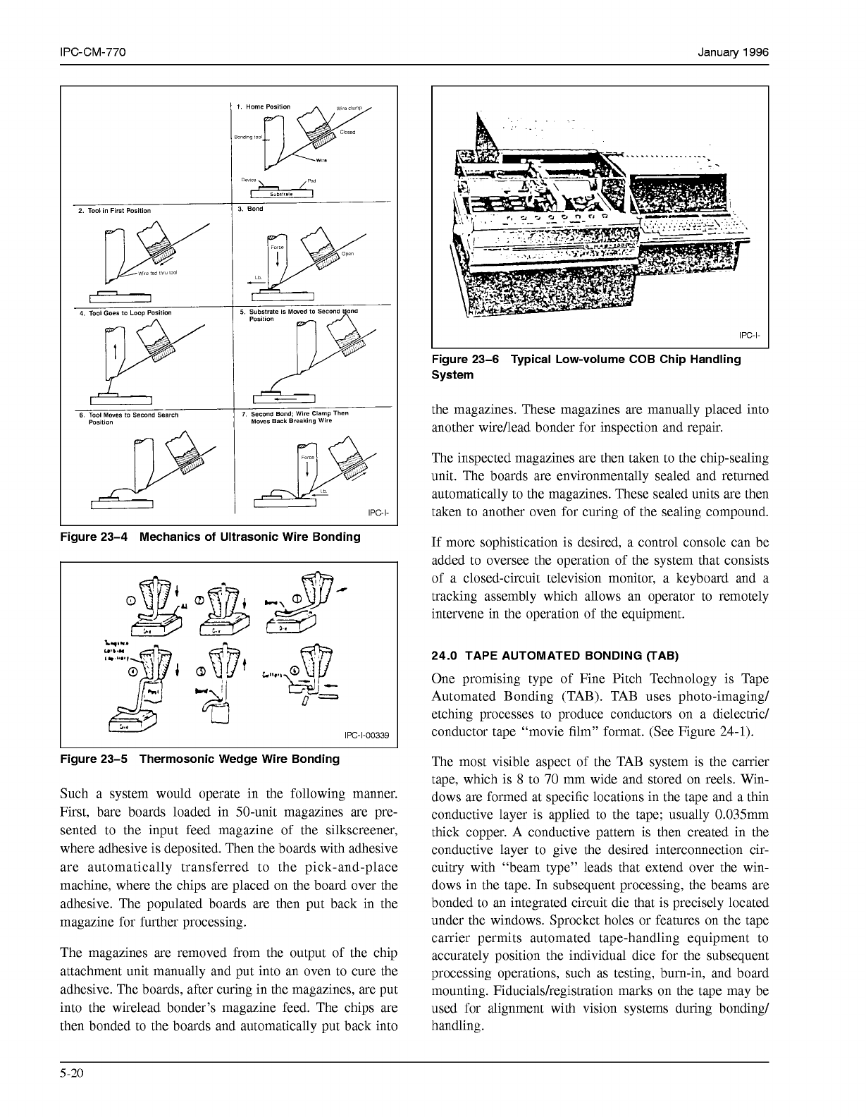
Figure 23-4 Mechanics
of
Ultrasonic Wire Bonding
IPC-1-00339
L
Figure 23-5 Thermosonic Wedge Wire Bonding
Such a system would operate in the following manner.
First, bare boards loaded in 50-unit magazines are pre-
sented to the input feed magazine of the silkscreener,
where adhesive is deposited. Then the boards with adhesive
are automatically transferred to the pick-and-place
machine, where the chips are placed on the board over the
adhesive. The populated boards are then put back in the
magazine for further processing.
The magazines are removed from the output of the chip
attachment unit manually and put into an oven to cure the
adhesive. The boards, after curing in the magazines, are put
into the wirelead bonder's magazine feed. The chips are
then bonded to the boards and automatically put back into
I
IPC-I-
Figure 23-6 Typical Low-volume COB Chip Handling
System
the magazines. These magazines are manually placed into
another wire/lead bonder for inspection and repair.
The inspected magazines are then taken to the chip-sealing
unit. The boards are environmentally sealed and returned
automatically to the magazines. These sealed units are then
taken to another oven for curing of the sealing compound.
If
more sophistication is desired, a control console can be
added to oversee the operation of the system that consists
of a closed-circuit television monitor, a keyboard and a
tracking assembly which allows an operator to remotely
intervene in the operation of the equipment.
24.0 TAPE AUTOMATED BONDING (TAB)
One promising type of Fine Pitch Technology is Tape
Automated Bonding (TAB). TAB uses photo-imaging/
etching processes to produce conductors on a dielectric/
conductor tape "movie film" format. (See Figure
24-1).
The most visible aspect of the TAB system is the carrier
tape, which is
8
to
70
mm wide and stored on reels. Win-
dows are formed at specific locations in the tape and a thin
conductive layer is applied to the tape; usually 0.035mm
thick copper. A conductive pattern is then created in the
conductive layer to give the desired interconnection cir-
cuitry with "beam type" leads that extend over the win-
dows in the tape. In subsequent processing, the beams are
bonded to an integrated circuit die that is precisely located
under the windows. Sprocket holes or features on the tape
carrier permits automated tape-handling equipment to
accurately position the individual dice for the subsequent
processing operations, such as testing, bum-in, and board
mounting. Fiducials/registration marks on the tape may be
used for alignment with vision systems during bonding/
handling.
5
-20
COPYRIGHT Association Connecting Electronics Industries
Licensed by Information Handling Services
COPYRIGHT Association Connecting Electronics Industries
Licensed by Information Handling Services