IPC-CM-770D-1996 - 第125页
January 1996 IPC-CM-770 The bumping process is typically performed at the water level. Water bumping may be performed by the semi- conductor manufacturer, independent bumping facilities, or by electronic companies produc…
IPC-CM-770
Januaty
1996
-
The rectangular TAB lead has a lower lead impedance -Dynamic bum-in of TAB packages is more costly in
and inductance than a round wire, thus enhancing high- both hardware tooling and bum-in.
speed applications.
-
Since leads are excised during the placement operations,
ration
is
much
the
Same
as
that
for
wire-bonded
wders.
A
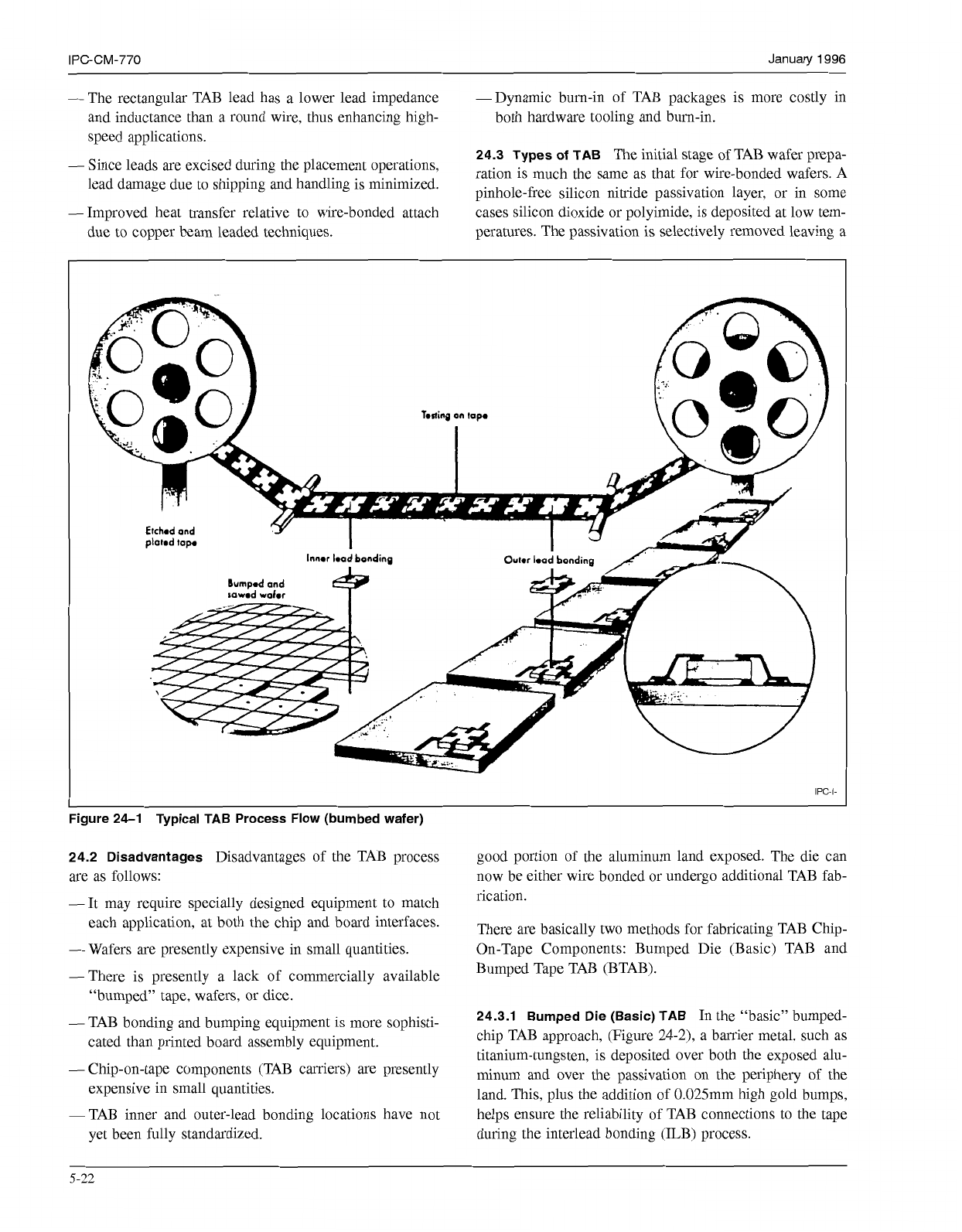
24.3 Types of TAB
The initial stage of TAB wafer prepa-
pinhole-free silicon nitride passivation layer, or in some
-
Improved heat transfer relative to wire-bonded attach cases silicon dioxide or polyimide, is deposited at low tem-
lead damage due to shipping and handling is minimized.
due to copper beam leaded techniques.
peratures. The passivation is selectively removed leaving a
IPC-I-
Figure 24-1 Typical TAB Process Flow (bumbed wafer)
24.2 Disadvantages
Disadvantages of the TAB process
are as follows:
-It may require specially designed equipment to match
each application, at both the chip and board interfaces.
-Wafers are presently expensive in small quantities.
-There is presently a lack of commercially available
“bumped” tape, wafers, or dice.
-
TAB bonding and bumping equipment is more sophisti-
cated than printed board assembly equipment.
-
Chip-on-tape components (TAB carriers) are presently
expensive in small quantities.
-TAB inner and outer-lead bonding locations have not
yet been fully standardized.
good portion of the aluminum land exposed. The die can
now be either wire bonded or undergo additional TAB fab-
rication.
There are basically two methods for fabricating TAB Chip-
On-Tape Components: Bumped Die (Basic) TAB and
Bumped Tape TAB (BTAB).
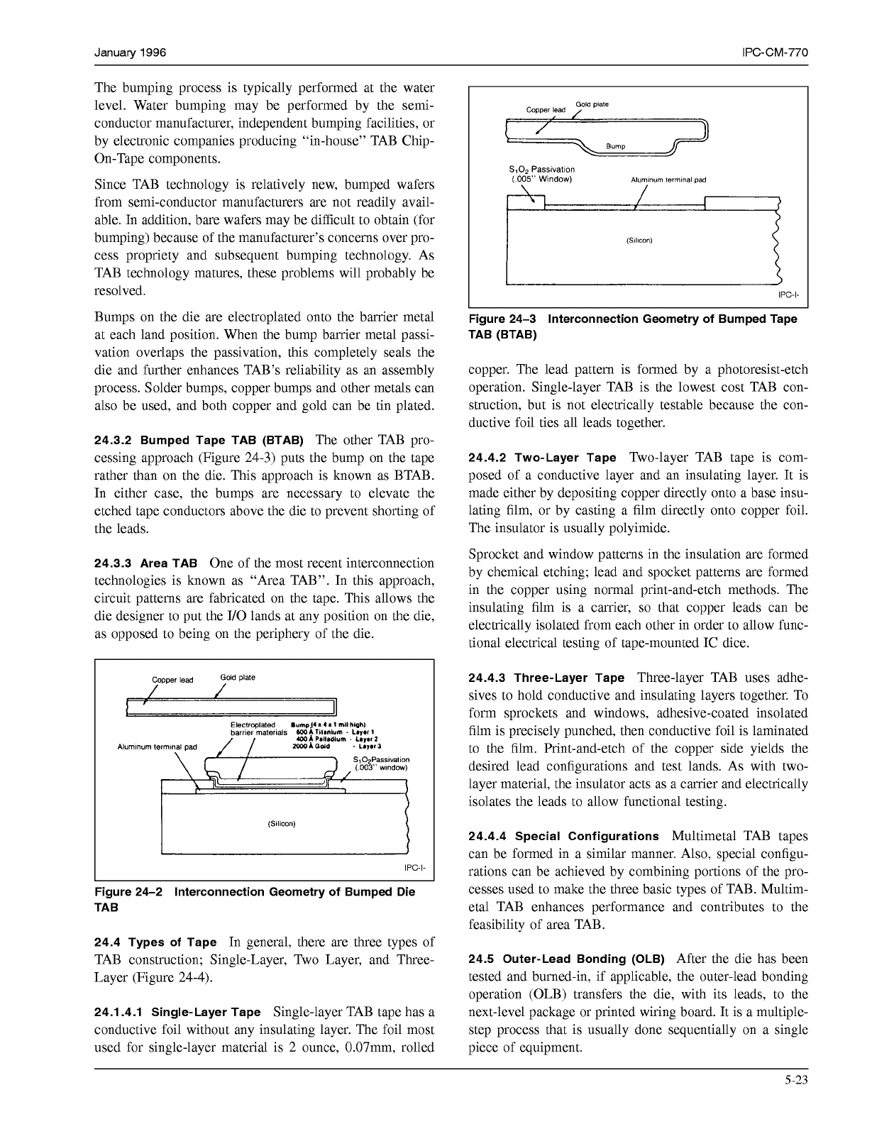
24.3.1 Bumped Die (Basic) TAB
In the “basic” bumped-
chip TAB approach, (Figure
24-2),
a barrier metal, such as
titanium-tungsten, is deposited over both the exposed alu-
minum and over the passivation on the periphery of the
land. This, plus the addition of 0.025mm high gold bumps,
helps ensure the reliability of TAB connections to the tape
during the interlead bonding (ILB) process.
5
-22
COPYRIGHT Association Connecting Electronics Industries
Licensed by Information Handling Services
COPYRIGHT Association Connecting Electronics Industries
Licensed by Information Handling Services
January
1996
IPC-CM-770
The bumping process is typically performed at the water
level. Water bumping may be performed by the semi-
conductor manufacturer, independent bumping facilities, or
by electronic companies producing “in-house” TAB Chip-
On-Tape components.
Since TAB technology is relatively new, bumped wafers
from semi-conductor manufacturers are not readily avail-
able. In addition, bare wafers may be difficult to obtain (for
bumping) because of the manufacturer’s concerns over pro-
cess propriety and subsequent bumping technology. As
TAB technology matures, these problems will probably be
resolved.
Bumps on the die are electroplated onto the barrier metal
at each land position. When the bump barrier metal passi-
vation overlaps the passivation, this completely seals the
die and further enhances TAB’S reliability as an assembly
process. Solder bumps, copper bumps and other metals can
also be used, and both copper and gold can be tin plated.
24.3.2 Bumped Tape TAB (BTAB)
The other TAB pro-
cessing approach (Figure 24-3) puts the bump on the tape
rather than on the die. This approach is known as BTAB.
In either case, the bumps are necessary to elevate the
etched tape conductors above the die to prevent shorting of
the leads.
24.3.3 Area TAB
One of the most recent interconnection
technologies is known as “Area TAB”. In this approach,
circuit patterns are fabricated on the tape. This allows the
die designer to put the I/O lands at any position on the die,
as opposed to being on the periphery of the die.
(
003’
wlndow)
(Slllcon)
IPC-I-
L
Figure 24-2 Interconnection Geometry of Bumped Die
TAB
24.4 Types of Tape
In general, there are three types of
TAB construction; Single-Layer, Two Layer, and Three-
Layer (Figure 24-4).
24.1.4.1 Single-Layer Tape
Single-layer TAB tape has a
conductive foil without any insulating layer. The foil most
used for single-layer material is 2 ounce, 0.07mm, rolled
Capper lead
Gold plate
/
Bump
S1O2
Passlvatlon
(005”
Window)
7
Alumlnum
lermlnal pad
(Slllcon)
IPC-I-
Figure 24-3 Interconnection Geometry of Bumped Tape
TAB (BTAB)
copper. The lead pattern is formed by a photoresist-etch
operation. Single-layer TAB is the lowest cost TAB con-
struction, but is not electrically testable because the con-
ductive foil ties all leads together.
24.4.2 Two-Layer Tape
Two-layer TAB tape is com-
posed of a conductive layer and an insulating layer. It is
made either by depositing copper directly onto a base insu-
lating film, or by casting a film directly onto copper foil.
The insulator is usually polyimide.
Sprocket and window patterns in the insulation are formed
by chemical etching; lead and spocket patterns are formed
in the copper using normal print-and-etch methods. The
insulating film is a carrier,
so
that copper leads can be
electrically isolated from each other in order to allow func-
tional electrical testing of tape-mounted IC dice.
24.4.3 Three-Layer Tape
Three-layer TAB uses adhe-
sives to hold conductive and insulating layers together. To
form sprockets and windows, adhesive-coated insolated
film is precisely punched, then conductive foil is laminated
to the film. Print-and-etch of the copper side yields the
desired lead configurations and test lands. As with two-
layer material, the insulator acts as a carrier and electrically
isolates the leads to allow functional testing.
24.4.4 Special Configurations
Multimetal TAB tapes
can be formed in a similar manner. Also, special configu-
rations can be achieved by combining portions of the pro-
cesses used to make the three basic types of TAB. Multim-
eta1 TAB enhances performance and contributes to the
feasibility of area TAB.
24.5 Outer-Lead Bonding (OLB)
After the die has been
tested and burned-in, if applicable, the outer-lead bonding
operation (OLB) transfers the die, with its leads, to the
next-level package or printed wiring board. It is a multiple-
step process that is usually done sequentially on a single
piece of equipment.
5-23
COPYRIGHT Association Connecting Electronics Industries
Licensed by Information Handling Services
COPYRIGHT Association Connecting Electronics Industries
Licensed by Information Handling Services
IPC-CM-770
Januaty
1996
1
Layer
0.061 mm [O.O024"l
Copper
PATTERM
IN
COPPER
FORMED
"""
"-""""
2
Laver
0.036 mm [O.O014"l
Copper
-7
PATTERNS
N
CUPPER
FORMED
7
IMAGE
-IN0
0.051 mm
10.002
1
Polyimide
1
3
Layer
kmrd
by
pmcWon
punching
Rnm.
In
POlylmM~
and
MM
0.036 mm
[0.00141
Copper
0.025
mm
[0.001
Adhesive
3-
"""""""_
"""""""_
"\
""""""
0.127 mm
[0.0057
Polyimide~
IPC-I-
Figure 24-4 1-, 2-, and
3
layer TAB Contructions
The first step in the OLB process is to excise the leaded die
from the carrier tape (Figure 24-5). The leaded die is then
transferred to the board in a way that precisely maintains
the original relationship of the die with respect to its tape
sprocket holes or to a vision system that positions leads to
lands. Thus, the die will be accurately placed on the board.
Depending on the TAB mounting configuration (see Figure
24-6) a secondary lead-forming operation may be included.
When required, care must be taken to assure that the leads
are shaped down to the board level without shorting them
against the electrically-active edge of the die.
A bonding operation is then performed on all interconnec-
tions by either thermocompression bonding, thermosonic
bonding, ultrasonic bonding, reflow, or the use of conduc-
tive adhesives. Leads may be bonded one-at-a-time using a
single-point border, or mass bonded using thermocompres-
sion, reflow and conductive adhesive techniques.
24.6 TAB Applications
Applications for TAB vary
widely depending on overall end-product packaging
IPC-I-
requirements. TAB is commonly used to attach chips to
Figure
24-5
Excising
of
the
leaded die
from
the
tape
both organic (printed wiring board) and inorganic
carrier
(ceramic) substrates. It has also been used in large assem-
blies, as well as in single-chip and multidie packages.
L
5-24
COPYRIGHT Association Connecting Electronics Industries
Licensed by Information Handling Services
COPYRIGHT Association Connecting Electronics Industries
Licensed by Information Handling Services