IPC-CM-770D-1996 - 第136页
IPC-CM-770 Januaty 1996 5-34 COPYRIGHT Association Connecting Electronics Industries Licensed by Information Handling Services COPYRIGHT Association Connecting Electronics Industries Licensed by Information Handling Serv…
January
1996
IPC-CM-770
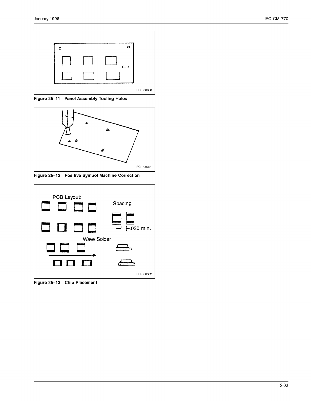
o
O
IPc-I-00050
L
Figure 25-11 Panel Assembly Tooling Holes
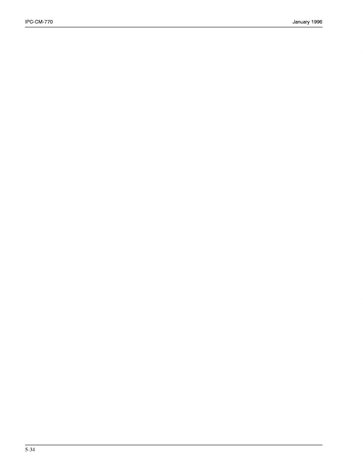
IPC-1-00361
L
Figure 25-12 Positive Symbol Machine Correction
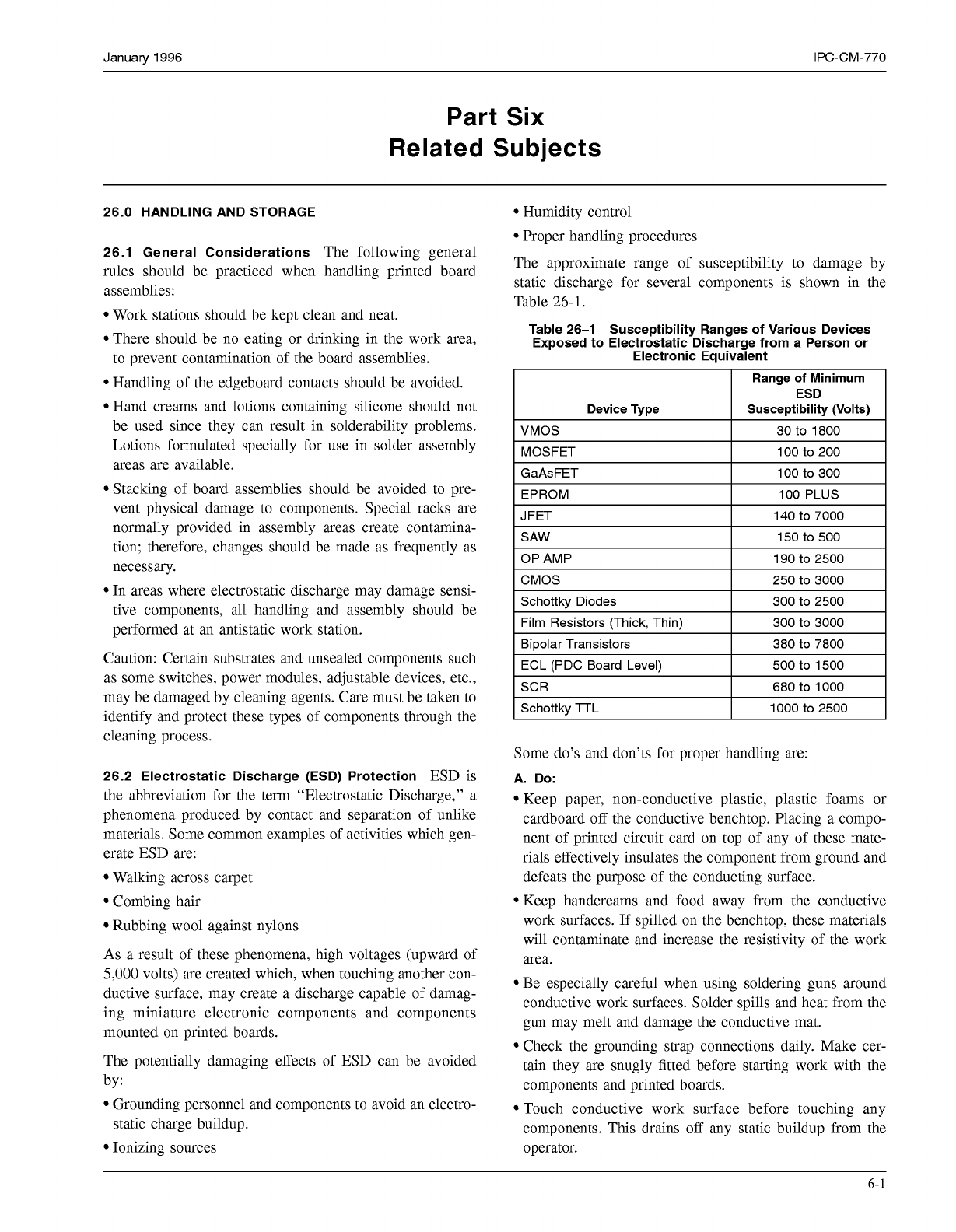
PCB
Layout:
Spacing
Wave Solder
-7
un
o
&%?I
IPC-1-00362
Figure 25-13 Chip Placement
5-33
COPYRIGHT Association Connecting Electronics Industries
Licensed by Information Handling Services
COPYRIGHT Association Connecting Electronics Industries
Licensed by Information Handling Services
IPC-CM-770
Januaty
1996
5-34
COPYRIGHT Association Connecting Electronics Industries
Licensed by Information Handling Services
COPYRIGHT Association Connecting Electronics Industries
Licensed by Information Handling Services
January 1996 IPC-CM-770
Part
Six
Related Subjects
26.0 HANDLING AND STORAGE
26.1 General Considerations
The following general
rules should be practiced when handling printed board
assemblies:
Work stations should be kept clean and neat.
There should be no eating or drinking in the work area,
to prevent contamination of the board assemblies.
Handling of the edgeboard contacts should be avoided.
Hand creams and lotions containing silicone should not
be used since they can result in solderability problems.
Lotions formulated specially for use in solder assembly
areas are available.
Stacking of board assemblies should be avoided to pre-
vent physical damage to components. Special racks are
normally provided in assembly areas create contamina-
tion; therefore, changes should be made as frequently as
necessary.
In areas where electrostatic discharge may damage sensi-
tive components, all handling and assembly should be
performed at an antistatic work station.
Caution: Certain substrates and unsealed components such
as some switches, power modules, adjustable devices, etc.,
may be damaged by cleaning agents. Care must be taken to
identify and protect these types of components through the
cleaning process.
26.2 Electrostatic Discharge (ESD) Protection
ESD is
the abbreviation for the term “Electrostatic Discharge,” a
phenomena produced by contact and separation of unlike
materials. Some common examples of activities which gen-
erate ESD are:
Walking across carpet
Combing hair
Rubbing wool against nylons
As
a result of these phenomena, high voltages (upward of
5,000
volts) are created which, when touching another con-
ductive surface, may create a discharge capable of damag-
ing miniature electronic components and components
mounted on printed boards.
The potentially damaging effects of ESD can be avoided
by:
Grounding personnel and components to avoid an electro-
static charge buildup.
Ionizing sources
Humidity control
Proper handling procedures
The approximate range of susceptibility to damage by
static discharge for several components is shown in the
Table
26-
1.
Table 26-1 Susceptibility Ranges of Various Devices
Exposed to Electrostatic Discharge from a Person or
Electronic Equivalent
Range
of
Minimum
ESD
Device Type
Susceptibility (Volts)
VMOS
1000 to 2500 Schottky TTL
680 to 1000 SCR
500 to 1500 ECL (PDC Board Level)
380 to
7800
Bipolar Transistors
300 to 3000 Film Resistors (Thick, Thin)
300 to 2500 Schottky Diodes
250 to 3000 CMOS
190 to 2500 OP AMP
150 to 500 SAW
140 to 7000 J FET
100 PLUS EPROM
100 to 300 GaAsFET
100 to 200 MOSFET
30 to 1800
Some do’s and don’ts for proper handling are:
A. Do:
Keep paper, non-conductive plastic, plastic foams or
cardboard off the conductive benchtop. Placing a compo-
nent of printed circuit card on top of any of these mate-
rials effectively insulates the component from ground and
defeats the purpose of the conducting surface.
Keep handcreams and food away from the conductive
work surfaces. If spilled on the benchtop, these materials
will contaminate and increase the resistivity of the work
area.
Be especially careful when using soldering guns around
conductive work surfaces. Solder spills and heat from the
gun may melt and damage the conductive mat.
Check the grounding strap connections daily. Make cer-
tain they are snugly fitted before starting work with the
components and printed boards.
Touch conductive work surface before touching any
components. This drains off any static buildup from the
operator.
6-
1
COPYRIGHT Association Connecting Electronics Industries
Licensed by Information Handling Services
COPYRIGHT Association Connecting Electronics Industries
Licensed by Information Handling Services