IPC-CM-770D-1996 - 第143页
January 1996 IPC-CM-770 26.4.2.2 Sequential Machines Provides for flexibility of programming placement of components-2,000 to 12,000 per hour. This level of automation allows for some compo- nent testing prior to the pla…
IPC-CM-770
Januaty
1996
Use
conduclive or anti.
bags and contamers
n
Usa
wrist
straps
and
I
z
Avord lead handimg
//
/
Pick
up
static
sensitive
devices
only by the
body.
Keep
Discharge personal static before
handling devices.
-
.
//
í2<
I
handling
work
stauon cmap
"
Avoid all plastic, vinyl and Styrofoam in the
work
area, except
anti-static
or
conductwe plastics.
Assemate
only
at gmundecl
work
s~atron
AVOIO
Charge generalron
Do
not
subject semconductors
to
shdlng movements over
any surface at any time.
IPC-I-O0301
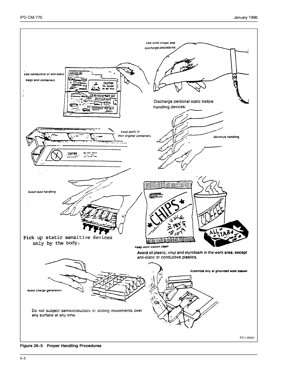
Figure
26-5
Proper Handling Procedures
6-6
COPYRIGHT Association Connecting Electronics Industries
Licensed by Information Handling Services
COPYRIGHT Association Connecting Electronics Industries
Licensed by Information Handling Services
January
1996
IPC-CM-770
26.4.2.2 Sequential Machines
Provides for flexibility of
programming placement of components-2,000 to 12,000
per hour. This level of automation allows for some compo-
nent testing prior to the placement the board.
26.4.2.3 Mass Placement Machines
Very high volume,
fairly dedicated machine used in the matrix of stocks or
multiplicity of tapes, which assembles a total circuit with
one or more codes of the machine, up to 200,000 compo-
nents per hour.
27.0 SOLDER-RELATED CONSIDERATIONS
This section details the printed wiring board, component,
surface finish, solderability, materials and various solder
process methodologies which can affect a manufacturer’s
soldering process yields.
27.1 General Considerations
The component mounting
technique used, the mounting sequence followed, and the
resultant assembly configuration will impact the soldering
techniques which can be applied for interconnection of
components and printed boards as well as the resultant
quality of the solder joints.
Excessively large clearances can result in draining of the
solder. Lead extension through the hole must be adequate
to ensure opportunity for a good solder joint and subse-
quent inspection but not
so
long as to cause interference
with tooling for subsequent processes or shorting to adja-
cent runs or assemblies.
Component and board considerations, independent of type,
that impact soldering should be considered.
27.1.1 Part Type
Mass soldering of assemblies is usually
done with either a solder wave or a reflow process with hot
air, radiation (infrared), condensation heat transfer or con-
ductive plate. Many leaded devices such as chip carriers
are currently not considered appropriate for wave soldering
and must be soldered with the reflow process. These
devices may appear on either the “solder source” or the
“solder destination” side of the board. All surface mounted
components mounted on the “solder destination” side must
be reflow soldered. Surface mounted devices with fewer
leads such as resistors, capacitors and small outline
(SO)
devices can be assembled with solder waves but the orien-
tation of the parts becomes important. Passive chips, SOTS,
SOICs and other components that can tolerate immersion
in the molten solder of a wave soldering machine may be
mounted on the “solder source” side of printed wiring
assemblies.
Through-hole mounted parts have the potential of resultant
lower quality solder joints if insulation material, potting
compound or other material is allowed to protrude into the
hole. Another characteristic of these devices is the ten-
dency to “raise” during the fluxinglwave soldering process
if not clinched or mechanically retained. For wave solder-
ing the through hole mounted devices should be mounted
on the “solder destination” side of the board. These
devices may not be compatible with reflow processes. The
component mass is another factor to be reviewed. Heavy
mass components require longer soldering times due to
their heatsinking characteristics.
27.1.2 LeadlLand Relationships
The leadless and
leaded termination provide different solder joint geometries
and the stress distribution is different in each case. If leads
are too short to protrude through the printed wiring board
or if the surface mount lands are too small, soldering may
become difficult. Printed board hole diameters must be con-
sidered for the type product to be used.
Costs and problems can be reduced if the designer selects
his devices prior to printed board design and then designs
the proper hole or land size, etc. “Non-standard’’ holes
and land patterns increase costs by making “non-
standard” devices mandatory.
Proper spacings can greatly increase automatic, semi-
automatic and manual speed of component placement.
Features should be, if possible, in straight line patterns
rather than random and they should be placed in such a
fashion that it will not be necessary to readjust the board
to the product.
Tooling holes should be placed as far apart as possible.
The designer must be certain no pre-mounted components
will interfere with the proper machine installation of
those devices that will subsequently be installed.
Printed board holes may be “non” plated or “through”
plated, drilled or punched, dependent upon the device
which will be eventually used and the quality required in
the final printed board. As a general rule, a drilled hole
will be more consistent in size and is advised where a
hole will eventually be plated through. Punched holes in
multilayer printed boards are not recommended since the
internal conductors may be damaged.
27.1.2.1 Leadless Component Terminations
This
geometry provides no compliancy, it results in a very rigid,
small lap solder joint depending on the reflowed solder
material system providing desired mechanical properties.
Visual inspection of the joint is limited to fillet appearance
on any castellation and pad extension. Cleaning is more
difficult with this geometry than with the leaded
termination.
27.1.2.2 Leaded Component Termination
This geom-
etry results in a narrow solder fillet. It provides compliancy
which can compensate for some degree of mismatch in
expansion between the component package and the sub-
strate. Visual inspection of solder joints is somewhat easier
6-7
COPYRIGHT Association Connecting Electronics Industries
Licensed by Information Handling Services
COPYRIGHT Association Connecting Electronics Industries
Licensed by Information Handling Services
IPC-CM-770
Januaty
1996
with this geometry. Cleaning operations are aided by this
geometry since it provides clearance between the bottom
of
the component and the substrate. Excess solder fillets on
this geometry can stiffen the lead and reduce any compli-
ancy advantage.
27.1.2.3 LeadlTermination Finishes
Finishes on the
leads of leaded component packages and on the metallized
terminations of leadless packages, whether for through-
hole or surface mounting, preserve and assure the solder-
ability of the interconnection surfaces without decreasing
the assembly yield or the attachment reliability. The large
number of solder joints, which frequently cannot be visu-
ally inspected not only because of their sheer numbers but
also because they are physically inaccessible, makes it
imperative that the solderability of the component I/Os be
positively assured prior to assembly. The lead finish that
accomplishes this is fused or reflowed tin or solder. The
solder coating can be obtained either by solder dipping or
tidlead plating with a subsequent reflow process. It might
be necessary to remove excess solder, which could inter-
fere with the assembly or socketing process, with a hot air
knife or similar method.
The above conditions expressly exclude gold plating, since
gold forms brittle intermetallics with the tin in the solder
causing solder joint reliability problems, and silver plating
since silver forms a brittle silver intermetallics. Caution
should be used when leads are coated with tin or tidead
plating without reflowing prior to assembly because the
plating does not always assure solderability. Organics
which are sometimes Co-deposited during the plating pro-
cess can also cause poor solderability.
In addition, some user specifications require fusing of tin
plate to eliminate the possibility of tin whisker growth.
The foregoing considerations are more critical for surface
mounting than for through-hole mounting. Through-hole
mounting provides considerable margin because of the
mechanical anchoring of the leads and the larger solder
volumes.
For devices which are exclusively destined for non-
soldered interconnections (sockets, connectors), the surface
finish coatings depend on the design of the mating contact,
the number of insertion/withdrawal cycles and the service
environment.
It should be noted that the reliability of a tin/lead applica-
tion can be increased by lubricating the contact surfaces
with proper contact lubricants. Lubricants prevent fret and
corrosion that may occur on tidead due to changing envi-
ronmental conditions. A suggested source for additional
information of recommended finishes is IPC-GH-850
Handbook of Interconnection Contact Finishes.
27.1.3 Component Placement
The orientation of com-
ponents on the assembly can have adverse effects on the
final solder joint quality. See the placement descriptions for
each of the component types in Sections
1
through
8.
27.1.4 Assembly Sequence.
See the assembly sequence
information in Sections
19
through 25.
27.2 Solderability
A successful solder joint requires cer-
tain conditions. Primarily, the surface to be joined must be
solderable; this is known as solderability.
Good solderability can improve production rates, increase
reliability, lower costs and improve joint appearance. Pro-
duction rates increase significantly if board solder joints do
not have to be reworked or touched up. Furthermore
manual touch up can damage printed boards. Therefore,
production increases as a result of reduced printed circuits
board scrappage due to touchup operations. Reliability
increases and costs drop for this same reason. With regard
to cost, obtaining better solderability definitely increases
cost; however, in most cases this added cost is less than the
cost of bad joints and will therefore actually save money.
The solderability of both component leads and printed
boards must be high to obtain an easily and well made
joint. Degradation of either part will impede the formation
of good solder joints. The solderability of printed wiring
boards should meet the requirements of J-STD-O03 and the
components should meet the requirements of J-STD-002.
The emphasis in the control of solderability has been
placed on component leads rather than on printed boards,
because of the following characteristics of components:
Longer storage times
More rigorous processing during manufacture
Greater variety of base materials
Lower cost compared to cost of reworking the PWB
Considerable work on solderability control has been
applied to printed wiring boards. This includes both testing
for solderability and improving the surfaces to be soldered.
Specific information on solderability can be found in:
J-STD-001, “Requirements for Soldered Electrical and
Electronic Assemblies” J-STD-002, “Solderability Tests
for Component Leads, Terminations, Lugs, Terminals and
Wires” J-STD-003, “Soderability Tests for Printed
Boards”
27.2.1 TinninglSolder Dipping
Component leads not
meeting the designated solderability requirements may pos-
sibly be reworked by tinningholder dipping, prior to sol-
dering. All portions of the wires or leads which come in
contact with the area to be soldered should be tinned. The
solder should penetrate to the inner strands of stranded
conductors. To permit inspection for nicks or cuts at the
point of insulation termination, solder and wicking should
not conceal the individual outer wire strands.
6-8
COPYRIGHT Association Connecting Electronics Industries
Licensed by Information Handling Services
COPYRIGHT Association Connecting Electronics Industries
Licensed by Information Handling Services