IPC-CM-770D-1996 - 第18页
IPC-CM-770 Januaty 1996 Electronic Grade, Soft Solder Alloys and Fluxed and Non- Fluxed Solid Solders for Electronic Soldering Applications 2.3 Department of Defense2 MIL-STD-1 O0 Engineering Drawing Practices MIL-STD-12…
January
1996
IPC-CM-770
m
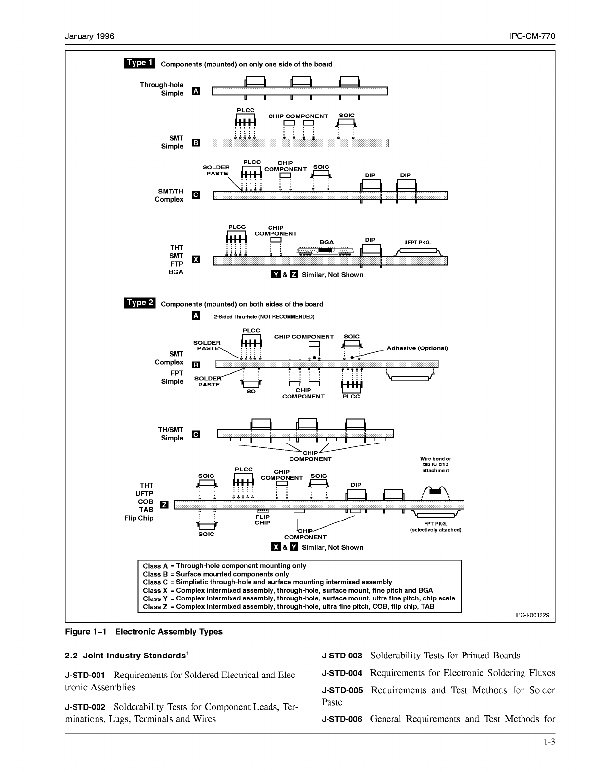
Components (mounted) on only one side of the board
Through-hole
Simple
I
uu
uu
uu
iz
o0
e
CHIP COMPONENT SOE
'OLDER
m
COMPONENT
PLCC CHIP
PASTE DIP DIP
..
SMTITH
. . . . .
. .
..
,,
"
"".
m&A&2
b
:
Complex
i:
II
li
i¡
,
I,
I,
II
u uu u
PLCC
CHID
BGA
&
Similar, Not Shown
m
Components (mounted) on both sides of the board
?-Sided Thru-hole (NOT RECOMMENDED)
SMT
Complex
FPT
Simple
THISMT
1:
i
'4
II
-CHIPe COMPONENT
Wire bond
or
tab IC chip
attachment
PLCC
CHIP
m
COMPONENT
THT
0
m
DIP
COB
Q
I
TAB
Flip Chip
UFTP
..
"".
..
"".
..
II
..
..
D
'"'2
"
"
I
U U
uuu
u u
CHIP
1
/
FLIP
W
"
..
..
-
FPT PKG.
U
SOlC
!CHI/
COMPONENT
&
Similar, Not Shown
(selectively attached)
Class A
=
Through-hole component mounting only
Class B
=
Surface mounted components only
Class C
=
Simplistic through-hole and surface mounting intermixed assembly
Class
X
=
Complex intermixed assembly, through-hole, surface mount, fine pitch and BGA
Class
Y
=
Complex intermixed assembly, through-hole, surface mount, ultra fine pitch, chip scale
Class
2
=
Complex intermixed assembly, through-hole, ultra fine pitch, COB, flip chip, TAB
IPC-1-001229
Figure 1-1 Electronic Assembly Types
2.2 Joint Industry Standards' J-STD-003
Solderability Tests for Printed Boards
J-STD-001
Requirements for Soldered Electrical and Elec-
J-STD-004
Requirements for Electronic Soldering Fluxes
tronic Assemblies
J-STD-005
Requirements and Test Methods for Solder
J-STD-002
Solderability Tests for Component Leads, Ter-
minations, Lugs, Terminals and Wires
J-STD-006
General Requirements and Test Methods for
Paste
1-3
COPYRIGHT Association Connecting Electronics Industries
Licensed by Information Handling Services
COPYRIGHT Association Connecting Electronics Industries
Licensed by Information Handling Services
IPC-CM-770
Januaty
1996
Electronic Grade, Soft Solder Alloys and Fluxed and Non-
Fluxed Solid Solders for Electronic Soldering Applications
2.3 Department of Defense2
MIL-STD-1
O0
Engineering Drawing Practices
MIL-STD-129
Marking for Shipment and Storage
MIL-STD-202
Test Methods for Electronic and Electrical
Component Parts
MIL-STD-454
Standard General Requirements for Elec-
tronic Equipment
MIL-STD-883
Test Methods and Procedures for Microelec-
tronics
MIL-STD-1344
Test Methods for Electrical Connectors
MIL-1-7444
Insulation Sleeving, Electrical, Flexible
MIL-C-11268
Parts, Materials, and Processes, Used in
Electronic Equipment
MIL-P-13949
Plastic Sheet, Laminated, Metal Clad, for
Printed Wiring Boards
MIL-S-1 9500
Semiconductor Devices, General Specifica-
tion
MIL-1-23053
Insulation Sleeving, Electrical, Heat Shrink-
able
MIL-P-28809
Printed Wiring Assemblies
MIL-M-3851
O
Semiconductor Devices, General Specifica-
tion
MIL-P-55110
Printed Wiring Boards
MIL-S-83502
Sockets, Plug-In Electronic Component,
Round Style
2.4 Electronic Industries Association3
JEDEC-95
JEDEC Registered and Standard Outlines for
Solid State Products
RS-167
Type Designation for Receiver Type Tube Sockets
RS-186-9E
Standard Test Methods for Passive Electronic
Component Parts-Method
9,
Solderability Rev. E
RS-192
Holder Outlines and Pin Connections for Quartz
Crystal Units
RS-198
Ceramic Dielectric Capacitors
RS-228
Fixed Electrolytic Tantalum Capacitors
RS-296
Lead Taping, Axial Components
RS-367
Dimensional and Electrical Characteristics Defin-
ing Receiver Type Sockets
RS-376
Fixed Film Dielectric Capacitors in Metallic and
Non-Metallic Cases for D.C. Application
RS-415
Dimensional and Electrical Characteristic Defin-
ing Dual-In-Line-Type Sockets
RS-428
Type Designation System for Microelectronic
Devices
RS-468
Lead Taping, Radial Components
RS-471
Symbol and Label for Electrostatic Sensitive
Devices
RS-481
Lead Taping, Leadless Components
RS-488
Sockets, Individual Lead Types (for Electrical and
Electronic Components)
2.5 American National Standards Institute4
ANSI Y-1 4.5
Dimensioning and Tolerancing
2.6 Underwriters Laboratories5
UL-1244
Electrical and Electronic Measuring and Testing
Equipment
2.7 American Society for Testing and Materials6
B25
Standard Nominal Diameters and Cross-Sectional
Areas of AWG Sizes of Solid Round Wires Used as Elec-
trical Conductors
F72
Gold Wire for Semiconductor Lead Bonding
F487
Fine Aluminum-
1
%
Silicon Wire for Semiconductor
Lead Bonding
D3295
Standard for PTFE Tubing
2.8 Other Documents
IEC-348
Safety Requirements for Electronic Measuring
Apparatus
FCC
Docket
20780
3.0 TERMS AND DEFINITIONS
Terms and definitions used herein are in accordance with
IPC-T-50 except as otherwise specified. Note: Any defini-
tion denoted with as asterisk
(*)
is a reprint of the defini-
tion defined in IPC-T-50.
2. Publications are available from Naval Publications and Form Center, 5801 Tabor Road, Philadelphia, PA 19120.
3. Electronic Industries Association, 2001
"I"
Street, NW, Washington, DC 20006.
4. American National Standards Institute, 11 W. 42nd St., New York, NY 10036.
5. Underwriters Laboratories, Inc., 333 Pfingsten Rd., Northbrook, IL 60062.
6. American Society for Testing and Materials, 1916 Race St., Philadelphia, PA 19103-1187.
1-4
COPYRIGHT Association Connecting Electronics Industries
Licensed by Information Handling Services
COPYRIGHT Association Connecting Electronics Industries
Licensed by Information Handling Services
January
1996
IPC-CM-770
3.1 *Assembly
A number of parts of subassemblies or
any combination thereof joined together.
Note: When this term is used in conjunction with other
terms listed herein, the following definitions shall prevail.
printed wiring assembly
-
An assembly that uses a
printed wiring board for component mounting and
interconnecting purposes.
multilayer printed wiring assembly
-
An assembly
that uses a multilayer printed wiring board for com-
ponent mounting and interconnecting purposes.
printed circuit assembly
-
An assembly that uses a
printed circuit board for component mounting and
interconnecting purposes.
multilayer printed circuit assembly
-
A multilayer
printed circuit board on which separately manufac-
tured components and parts have been added.
printed board assembly
-
An assembly of several
printed circuit assemblies or printed wiring assem-
blies, or both.
3.2 *Base Material
The insulating material upon which
the conductor pattern may be formed. (The base material
may be rigid or flexible or both. It may be a dielectric sheet
or insulated metal sheet.
3.3 *Castellations
A recessed metallized features on the
edge of a leadless chip carrier that is used to interconnect
conducting surfaces or planes within or on the chip carrier.
3.4 *Chip Carrier
A low-profile, usually square, surface
mount component semiconductor package whose die cavity
or die mounting area is a large fraction of the package size
and whose external connections are usually on all four
sides of the packaged. (It may be leaded or leadless.)
3.5 *Clinched Leads
A component lead that is inserted
through a hole in a printed board and is then formed in
order to retain the component in place and in order to make
metal-to-metal contact with a land prior to soldering. (See
also “Partially-Clinched Lead.”)
3.6 Coefficient of Thermal Expansion (CTE)
The linear
thermal expansion per unit change in temperature.
3.7 *Coefficient of Thermal Expansion Mismatch
(CTE)
The linear dimensional change of a material per
unit change in temperature. (See also “Thermal Expansion
Mismatch.”)
3.8 *Component
The individual part or combination of
parts that, when together, perform a design function(s).
(See also “Discrete Component.”)
3.9 *Component Lead Hole
A hole used for the attach-
ment and electrical connection of component terminations,
including pins and wires, to the printed board.
3.10 *Component Mounting Site
A location on a pack-
aging and interconnection structure that consists of a land
pattern and conductor fan out to additional lands for test-
ing or vias that are associated with the mounting of a single
component.
3.11 *Conductive Pattern
The configuration or design
of the conductive material on the base material. (Includes
conductors, lands, vias, heatsinks and passive components
when these are an integral part of the printed board manu-
facturing process.)
3.12 *Conductor
A single conductive path in a conduc-
tive pattern.
3.13 *Constraining Core
A supporting plane that is
internal to a packaging and interconnecting structure.
3.14 *Double-Sided Assembly
A packaging and inter-
connecting structure with components mounted on both the
primary and secondary sides. (Also see “Single-Sided
Assembly.”)
3.1
5
*Dual lnline Package (DIP)
A basically -rectangular
component package that has a row of leads extending from
each of the longer sides of its body that are formed at right
angles to a plan that is parallel to the base of its body.
3.1 6 *Edge Board Connector
A connector designed spe-
cifically for making nonpermanent interconnections
between the edge-board contacts on a printed board.
3.17 *Flat Pack
A rectangular component package that
has a row of leads extending from each of the longer sides
of its body that are parallel to the base of its body.
3.1 8 *Footprint
(see preferred term “Land Pattern”)
3.1 9 *Grid
An orthogonal network of two sets of parallel
equidistant lines used for locating points on a printed
board.
3.20 Integrated Circuit (IC)
An assembly of miniature
electronic components simultaneously produced in batch
processing, on or within a single substrate to perform an
electronic circuit function.
1-5
COPYRIGHT Association Connecting Electronics Industries
Licensed by Information Handling Services
COPYRIGHT Association Connecting Electronics Industries
Licensed by Information Handling Services