IPC-CM-770D-1996 - 第26页
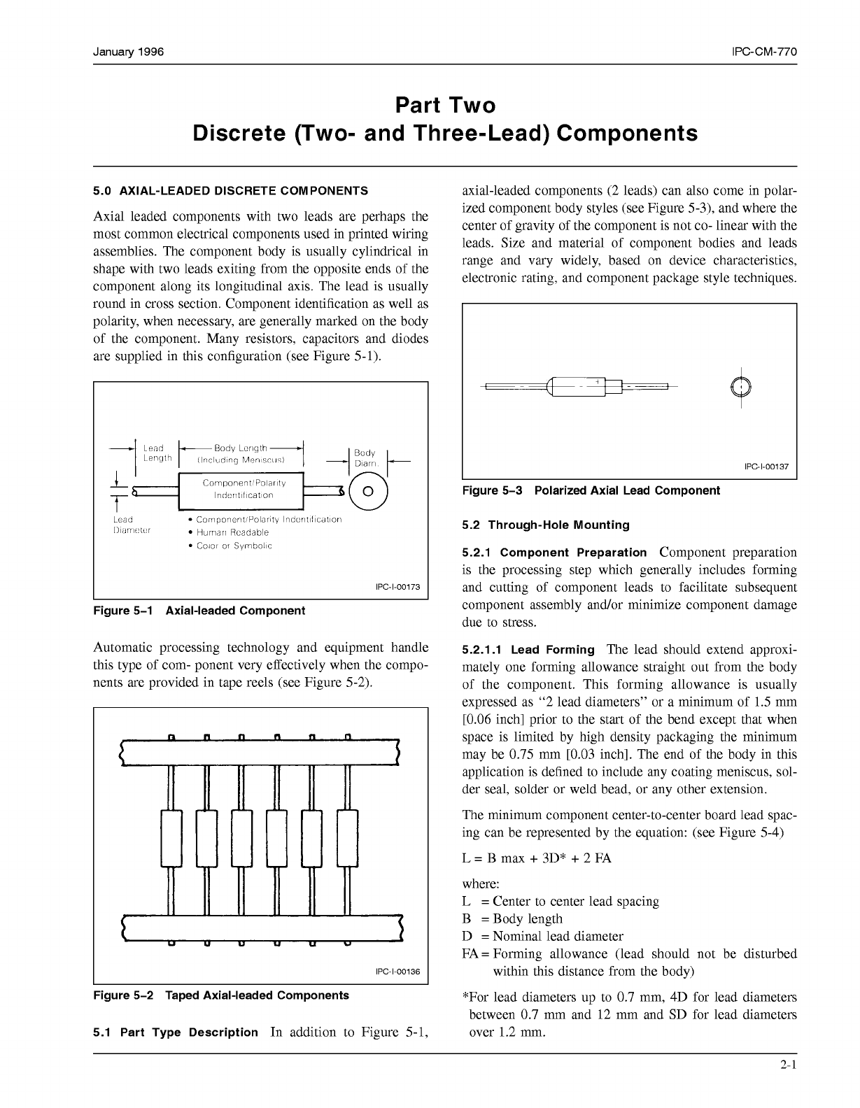
IPC-CM-770 Januaty 1996 Figure 5-4 The value of "L" is usually adjusted upward to coincide with the grid used. The total length of both leads should not exceed 25 mm in length unless this component is mechanica…
January
1996
IPC-CM-770
Part Two
Discrete (Two- and Three-Lead) Components
5.0 AXIAL-LEADED DISCRETE COMPONENTS
Axial leaded components with two leads are perhaps the
most common electrical components used in printed wiring
assemblies. The component body is usually cylindrical in
shape with two leads exiting from the opposite ends of the
component along its longitudinal axis. The lead is usually
round in cross section. Component identification as well as
polarity, when necessary, are generally marked on the body
of the component. Many resistors, capacitors and diodes
are supplied in this configuration (see Figure
5-1).
IPC-1-00173
I
L
Figure 5-1 Axial-leaded Component
Automatic processing technology and equipment handle
this type of com- ponent very effectively when the compo-
nents are provided in tape reels (see Figure 5-2).
I
3
\
L
U
U
U
U U
v
IPC-1-00136
I
L
Figure 5-2 Taped Axial-leaded Components
5.1 Part Type Description
In addition to Figure
5-1,
axial-leaded components (2 leads) can also come in polar-
ized component body styles (see Figure 5-3), and where the
center of gravity of the component is not CO- linear with the
leads. Size and material of component bodies and leads
range and vary widely, based on device characteristics,
electronic rating, and component package style techniques.
Figure 5-3 Polarized Axial Lead Component
5.2 Through-Hole Mounting
5.2.1 Component Preparation
Component preparation
is the processing step which generally includes forming
and cutting of component leads to facilitate subsequent
component assembly and/or minimize component damage
due to stress.
5.2.1.1 Lead Forming
The lead should extend approxi-
mately one forming allowance straight out from the body
of the component. This forming allowance is usually
expressed as “2 lead diameters” or a minimum of
1.5
mm
[0.06
inch] prior to the start of the bend except that when
space is limited by high density packaging the minimum
may be
0.75
mm [0.03 inch]. The end of the body in this
application is defined to include any coating meniscus, sol-
der seal, solder or weld bead, or any other extension.
The minimum component center-to-center board lead spac-
ing can be represented by the equation: (see Figure 5-4)
L=Bmax+3D*+2FA
where:
L
=
Center to center lead spacing
B
=
Body length
D
=
Nominal lead diameter
FA
=
Forming allowance (lead should not be disturbed
within this distance from the body)
*For lead diameters up to
0.7
mm, 4D for lead diameters
between
0.7
mm and 12 mm and SD for lead diameters
over 1.2 mm.
2-
1
COPYRIGHT Association Connecting Electronics Industries
Licensed by Information Handling Services
COPYRIGHT Association Connecting Electronics Industries
Licensed by Information Handling Services
IPC-CM-770
Januaty
1996
Figure 5-4
The value of
"L"
is usually adjusted upward to coincide
with the grid used. The total length of both leads should
not exceed
25
mm in length unless this component is
mechanically supported to the mounting base.
5.2.1.2 Minimum Inside Bend Radius
The minimum
inside bend radius of a single
90
bend of a component lead
should be in accordance with Figure
5-5.
-
Straightfor2
11
[O.(u,hch]
,
diameters, but not
le88
than
0.76mm
A.
Standard bend
I-Dia.
B.
Welded bend
1.22mm
[0.048
inches] and larger
2
diameters
IPC-I-O0025
L
Figure
5-5
Lead Diameter Versus Bend Radius
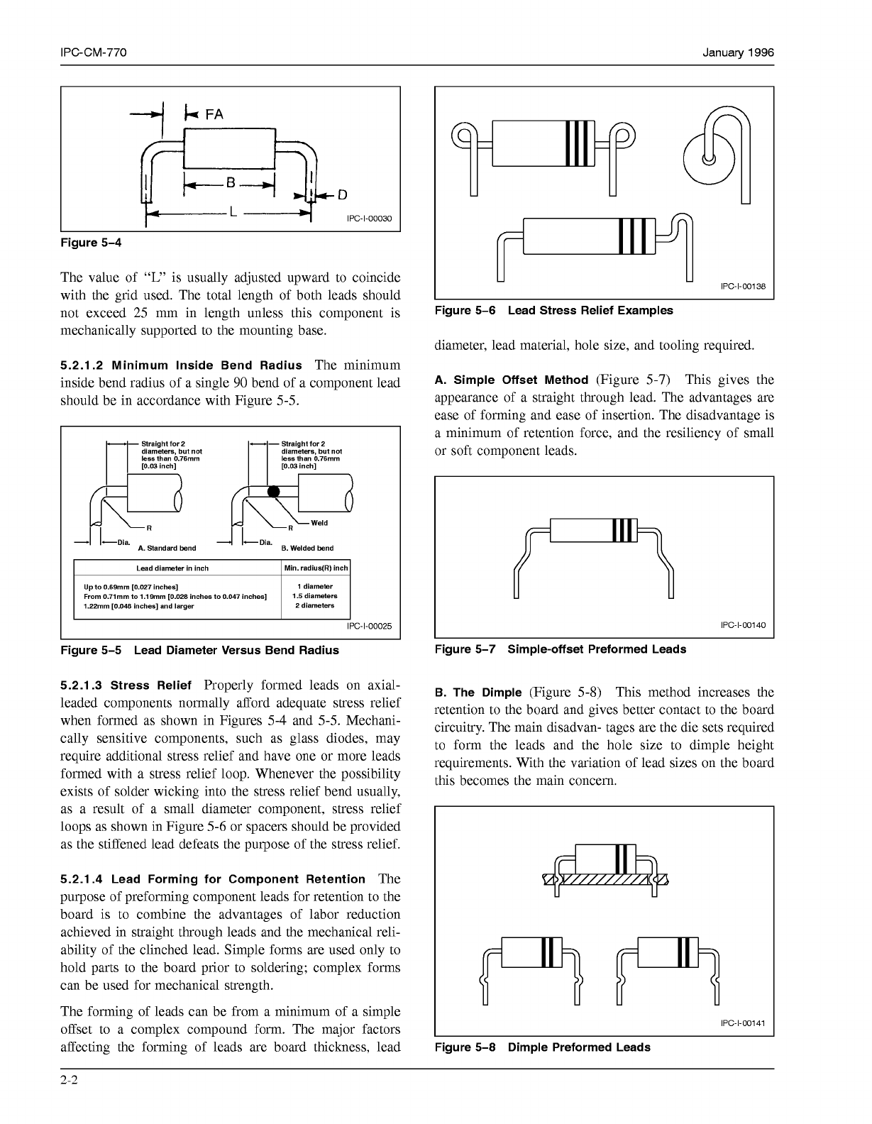
5.2.1.3 Stress Relief
Properly formed leads on axial-
leaded components normally afford adequate stress relief
when formed as shown in Figures
5-4
and
5-5.
Mechani-
cally sensitive components, such as glass diodes, may
require additional stress relief and have one or more leads
formed with a stress relief loop. Whenever the possibility
exists of solder wicking into the stress relief bend usually,
as a result of a small diameter component, stress relief
loops as shown in Figure
5-6
or spacers should be provided
as the stiffened lead defeats the purpose of the stress relief.
5.2.1.4 Lead Forming for Component Retention
The
purpose of preforming component leads for retention to the
board is to combine the advantages of labor reduction
achieved in straight through leads and the mechanical reli-
ability of the clinched lead. Simple forms are used only to
hold parts to the board prior to soldering; complex forms
can be used for mechanical strength.
The forming of leads can be from a minimum of a simple
offset to a complex compound form. The major factors
affecting the forming of leads are board thickness, lead
m
IPC-1-00138
Figure
5-6
Lead Stress Relief Examples
diameter, lead material, hole size, and tooling required.
A.
Simple Offset Method
(Figure
5-7)
This gives the
appearance of a straight through lead. The advantages are
ease of forming and ease of insertion. The disadvantage is
a minimum of retention force, and the resiliency of small
or soft component leads.
IPC-I-O0140
Figure
5-7
Simple-offset Preformed Leads
B. The Dimple
(Figure
5-8)
This method increases the
retention to the board and gives better contact to the board
circuitry. The main disadvan- tages are the die sets required
to form the leads and the hole size to dimple height
requirements. With the variation of lead sizes on the board
this becomes the main concern.
IPC-1-00141
Figure 5-8 Dimple Preformed Leads
2-2
COPYRIGHT Association Connecting Electronics Industries
Licensed by Information Handling Services
COPYRIGHT Association Connecting Electronics Industries
Licensed by Information Handling Services
January
1996
IPC-CM-770
C. Compound Forms
(Figure
5-9)
This method gives the
best retention and has the advantage of near clinched lead
reliability. Disadvantages in- clude complex tooling
required to form leads and the need for tighter control of
hole sizes.
B
5
IPC-I-O0142
L
Figure 5-9 Compound Preformed Leads
D.
Combinations
(Figure
5-10)
These are used to gain
the advantages of the above methods and overcome some
of the disadvantages.
mm
IPC-1-00143
Figure 5-10 Combination Preformed Leads
5.2.2 Land Patterns
Land patterns must consider
minimudmaximum lead spacing requirements. Standard
land spacing patterns should be established for the purpose
of uniformity of assemblies and the practical use of assem-
bly tools and equipment. Spacing(s) should be located to
accommodate automatic assembly-and “bed-of-nails’’ type
of testing equipment, (usually
2.5
mm increments-i.e.,
7.5
mm,
10
mm,
12.5
mm, etc.).
Land patterns for unsupported holes should have more sol-
derable area than that for supported holes for a stronger
joint after soldering. The optimum dimension is dependent
on the device and its mounting characteristics.
The most common geometry is the round land with a cen-
tered hole. Square lands with centered holes are sometimes
used to indicate polarity for polarized components.
Additional information for holeAand requirements can be
found in Section
21
(Through-Hole Mounting Techniques).
5.2.3 Lead Configuration After Assembly
5.2.3.1 Straight Through Leads
Partially clinched leads,
where the components are secured with only limited move-
ment and the leads are in contact with the land patterns,
shall be considered as being straight through leads.
Lead projection from an unsupported hole should be
0.5
mm minimum. Lead bend at the solder side is allowed to
the extent that minimum electrical clearances are main-
tained from all conductive surfaces with different electrical
potential.
Lead projection from a supported hole should extend at
least beyond the bottom surface of the board to the extent
that, as a minimum, the lead contour is discernible after
soldering.
Lead projection of specially preformed leads for compo-
nent retention without clinching can be used to eliminate
the need for post-soldering lead cutting.
Additional information for lead projections can be found in
Section
21.
5.2.3.2 Clinched Leads
Clinched leads are leads that are
formed to the land within one lead diameter of the land for
both supported or unsupported holes. Leads should not
extend beyond the land to reduce, by more than half, the
electrical spacing to any adjacent conductive patterns.
5.2.4 Mounted Component Configuration
5.2.4.1 Lead Spacing
Where practical, components with
similar physical dimensions should have the same lead
spacing and be on the design grid.
5.2.4.2 Component Body
Through-hole components
should be mounted on one side of the board only. Com-
ponents should not be mounted across or on top of vias,
exposed conductive patterns and other components. (See
Figure
5
-
1 1
.)
Component bodies should not be closer than
1.5
mm from
the board edge. (See Figure
5-12.)
Resistors with power rating above
1
watt should be
mounted with a clearance of at least 0.5mm from the board
surface.
5.2.4.3 Component Orientation
Horizontally mounted
components should be oriented in either of the two board
axes preferably with component identification in the same
direction. (See Figure
5-13.)
The body of the component
should be approximately centered between the lead spac-
ing. In general, components with cylindrical bodies should
be in direct contact to the mounting base. Density of com-
ponent mount should consider clearance needed for compo-
nent assembly, electrical clearance, and ease of rework.
(See Figure
5-14.)
5.2.4.4 Vertical Mounting
Components mounted perpen-
dicular to printed wiring boards should be installed with a
2-3
COPYRIGHT Association Connecting Electronics Industries
Licensed by Information Handling Services
COPYRIGHT Association Connecting Electronics Industries
Licensed by Information Handling Services