IPC-CM-770D-1996 - 第31页
January 1996 IPC-CM-770 6.2.2 Land Patterns Information on land patterns fol- lows that cited in Section 5.2.2 for axial-leaded compo- nents. IPC-1-00183 I Figure 6-5 Stress Relief Leads 6.2.3 Vertical Mounting Component…
IPC-CM-770
Januaty
1996
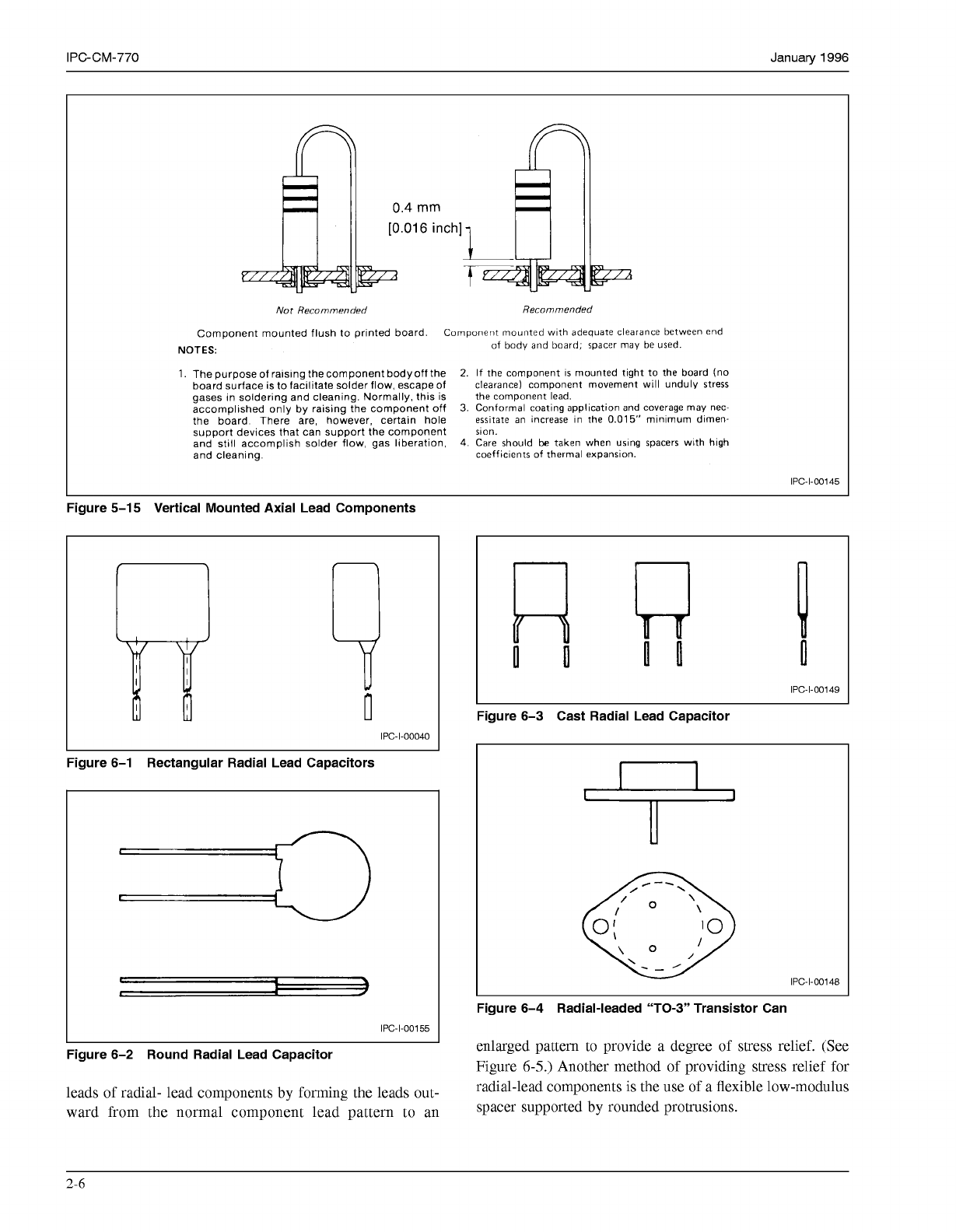
0.4
mm
Not
Recommended Recommended
Component mounted flush to prlnted board. Component mounted wlth adequate clearance between end
NOTES:
1.
The purpose of ralslng the component body off the
2.
If the component
IS
mounted tight to the board
(no
board surface is to facilitate solder flow, escape of
clearance) component movement will unduly Stress
gases in soldering and cleaning. Normally, this
is
the component lead.
accomplished only by raising the component
off
3.
Conformal coating
application
and coverage may nec-
the board There are, however, certain hole
essitate
an increase
In
the
0.015’’
mlnlmum
dlmen-
support devices that can support the component
son.
and still accomplish solder flow, gas liberation,
4.
Care should
be
taken when uslng spacers with
hlgh
and cleaning.
coefficlents of thermal expansion.
of
body and board; spacer may
be
used.
IPC-1-00145
Figure 5-1
5
Vertical Mounted Axial Lead Components
IPc-I-00040
Figure 6-1 Rectangular Radial Lead Capacitors
1
IPC-1-00155
Figure 6-2 Round Radial Lead Capacitor
leads of radial- lead components by forming the leads out-
ward from the normal component lead pattern to an
I
IPC-1-00149
I
Figure 6-3 Cast Radial Lead Capacitor
0
\
/
r”
IPC-1-00148
Figure 6-4 Radial-leaded “TO-3” Transistor Can
enlarged pattern to provide a degree of stress relief. (See
Figure
6-5.)
Another method of providing stress relief for
radial-lead components is the use of a flexible low-modulus
spacer supported by rounded protrusions.
2-6
COPYRIGHT Association Connecting Electronics Industries
Licensed by Information Handling Services
COPYRIGHT Association Connecting Electronics Industries
Licensed by Information Handling Services
January
1996
IPC-CM-770
6.2.2 Land Patterns
Information on land patterns fol-
lows that cited in Section
5.2.2
for axial-leaded compo-
nents.
IPC-1-00183
I
Figure 6-5 Stress Relief Leads
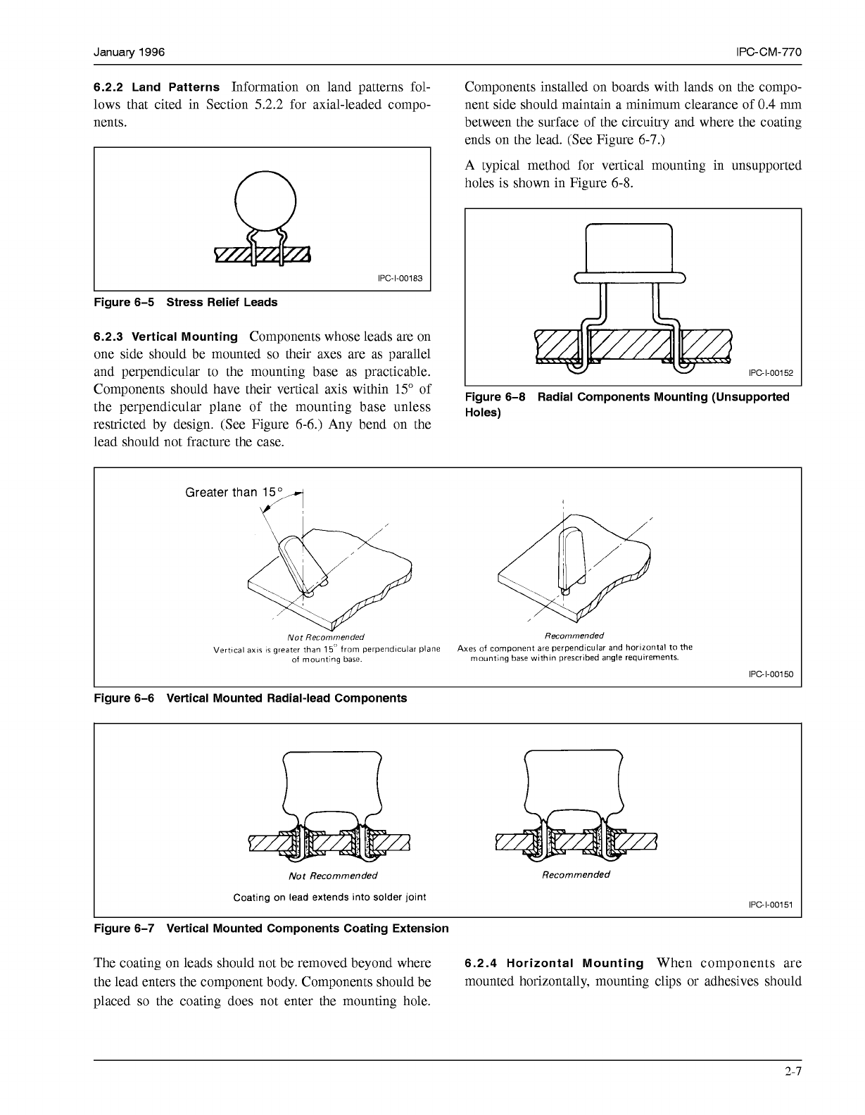
6.2.3 Vertical Mounting
Components whose leads are on
one side should be mounted
so
their axes are as parallel
and perpendicular to the mounting base as practicable.
Components should have their vertical axis within
15"
of
the perpendicular plane of the mounting base unless
restricted by design. (See Figure
6-6.)
Any bend on the
lead should not fracture the case.
Components installed on boards with lands on the compo-
nent side should maintain a minimum clearance of
0.4
mm
between the surface of the circuitry and where the coating
ends on the lead. (See Figure
6-7.)
A typical method for vertical mounting in unsupported
holes is shown in Figure
6-8.
IPC-1-00152
Figure 6-8 Radial Components Mounting (Unsupported
Holes)
Greater than
15
Not
Recommended
Recornmended
Vertical
axis
is
greater than
15''
from perpendlcular plane Axes
of
component are perpendicular and
horizontal
to the
of
mountlng base. mounting base wlthln prescrlbed angle requirements.
IPC-1-00150
Figure 6-6 Vertical Mounted Radial-lead Components
Not
Recommended
Coating on lead extends into solder joint
Recommended
IPC-1-00151
Figure 6-7 Vertical Mounted Components Coating Extension
The coating on leads should not be removed beyond where
6.2.4 Horizontal Mounting
When components are
the lead enters the component body. Components should be mounted horizontally, mounting clips or adhesives should
placed
so
the coating does not enter the mounting hole.
2-7
COPYRIGHT Association Connecting Electronics Industries
Licensed by Information Handling Services
COPYRIGHT Association Connecting Electronics Industries
Licensed by Information Handling Services
IPC-CM-770
Januaty
1996
be used. A typical method of mounting a component of this
type is shown in Figure 6-9.
I I
'C-
I
-00185
Figure 6-9 Horizontal Mounting of Radial Leaded
Component
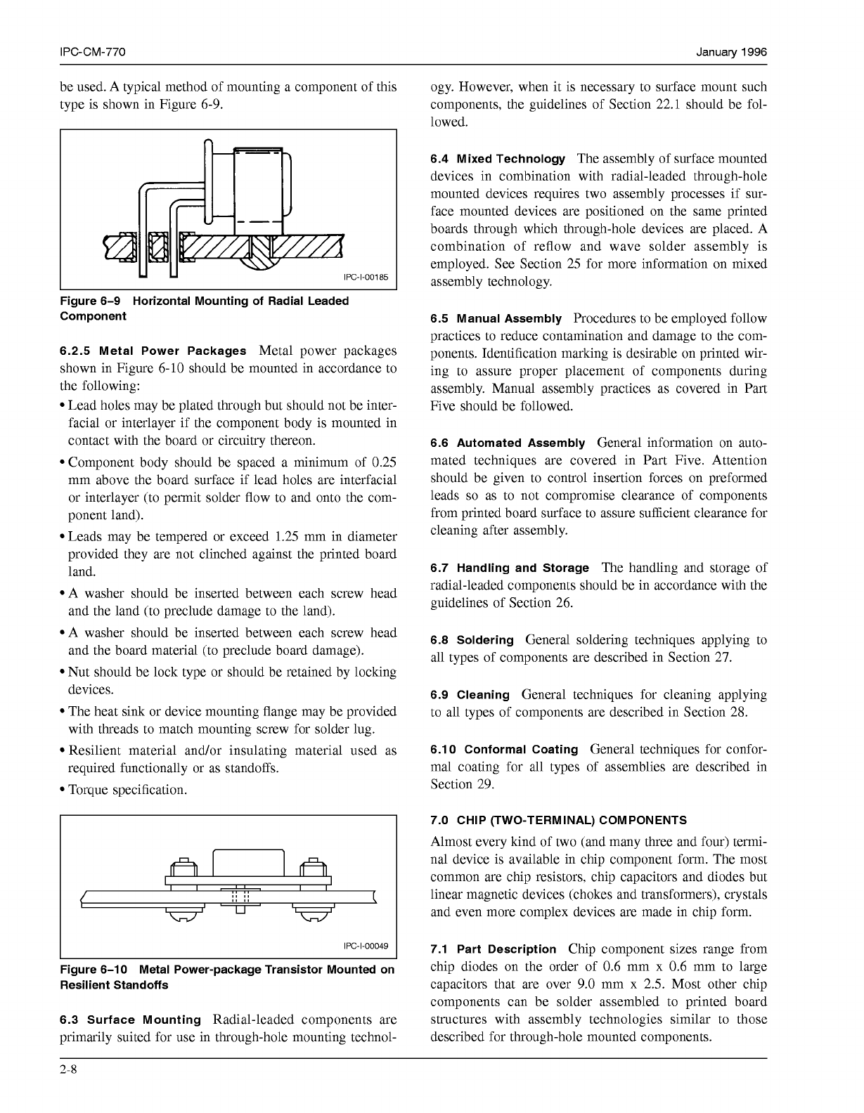
6.2.5 Metal Power Packages
Metal power packages
shown in Figure 6-10 should be mounted in accordance to
the following:
Lead holes may be plated through but should not be inter-
facial or interlayer if the component body is mounted in
contact with the board or circuitry thereon.
Component body should be spaced a minimum of 0.25
mm above the board surface if lead holes are interfacial
or interlayer (to permit solder flow to and onto the com-
ponent land).
Leads may be tempered or exceed 1.25 mm in diameter
provided they are not clinched against the printed board
land.
A washer should be inserted between each screw head
and the land (to preclude damage to the land).
A washer should be inserted between each screw head
and the board material (to preclude board damage).
Nut should be lock type or should be retained by locking
devices.
The heat sink or device mounting flange may be provided
with threads to match mounting screw for solder lug.
Resilient material and/or insulating material used as
required functionally or as standoffs.
Torque specification.
IPC-1-00049
I
L
Figure 6-1
O
Metal Power-package Transistor Mounted on
Resilient Standoffs
6.3 Surface Mounting
Radial-leaded components are
primarily suited for use in through-hole mounting technol-
ogy. However, when it is necessary to surface mount such
components, the guidelines of Section 22.1 should be fol-
lowed.
6.4 Mixed Technology
The assembly of surface mounted
devices in combination with radial-leaded through-hole
mounted devices requires two assembly processes if sur-
face mounted devices are positioned on the same printed
boards through which through-hole devices are placed. A
combination of reflow and wave solder assembly is
employed. See Section 25 for more information on mixed
assembly technology.
6.5 Manual Assembly
Procedures to be employed follow
practices to reduce contamination and damage to the com-
ponents. Identification marking is desirable on printed wir-
ing to assure proper placement of components during
assembly. Manual assembly practices as covered in Part
Five should be followed.
6.6 Automated Assembly
General information on auto-
mated techniques are covered in Part Five. Attention
should be given to control insertion forces on preformed
leads
so
as to not compromise clearance of components
from printed board surface to assure sufficient clearance for
cleaning after assembly.
6.7 Handling and Storage
The handling and storage of
radial-leaded components should be in accordance with the
guidelines of Section 26.
6.8 Soldering
General soldering techniques applying to
all types of components are described in Section 27.
6.9 Cleaning
General techniques for cleaning applying
to all types of components are described in Section 28.
6.1
O
Conformal Coating
General techniques for confor-
mal coating for all types of assemblies are described in
Section 29.
7.0 CHIP (TWO-TERMINAL) COMPONENTS
Almost every kind of two (and many three and four) termi-
nal device is available in chip component form. The most
common are chip resistors, chip capacitors and diodes but
linear magnetic devices (chokes and transformers), crystals
and even more complex devices are made in chip form.
7.1 Part Description
Chip component sizes range from
chip diodes on the order of 0.6 mm x 0.6 mm to large
capacitors that are over 9.0 mm x 2.5. Most other chip
components can be solder assembled to printed board
structures with assembly technologies similar to those
described for through-hole mounted components.
2-8
COPYRIGHT Association Connecting Electronics Industries
Licensed by Information Handling Services
COPYRIGHT Association Connecting Electronics Industries
Licensed by Information Handling Services