IPC-CM-770D-1996 - 第36页
IPC-CM-770 Januaty 1996 reflowed. Automated board handling facilitates precise and rapid movement of assemblies through the process. 7.7 Handling and Storage The handling and storage of chip components should be in accor…
January
1996
IPC-CM-770
Printed Wiring Board
(Pm)
lands for the solder assembly
of rectangular chip components should be approximately
the same width as the component terminations, Lands that
are significantly narrower than the component do not pro-
vide adequate space for the formation of good fillets and
lands that are much wider than the part waste space. Lands
that are either too narrow or too wide can allow too much
lateral motion of the part.
If the components are attached to the substrate with adhe-
sive before soldering the size and shape of the land is less
critical than when the components are held in place with
solder paste and reflowed. Very wide or very narrow lands
are undesirable for solder paste reflow assembly because
they allow excessive motion of the component during the
reflow process. Lands for cylindrical (MELF) components
should have a width approximately equal to the diameter of
the component. Adhesive bonding of cylindrical parts to
the substrate is recommended for both wave and reflow
soldering.
The length of the bonding land for rectangular chips must
be adequate to provide a satisfactory fillet at the allowable
extremes of the tolerances on board, placement and com-
ponent dimensions. For components that are bonded to the
substrate for wave soldering, the primary limitations on the
length of the land are solder process restrictions. Either the
length of the land must be restricted or other measures
must be taken to prevent excessive solder build-up on the
end terminations of the components. Excess solder on the
end terminations can damage the components.
When parts are held to the lands with solder paste and then
reflow soldered, the lands must also be restricted to limit
the motion of the part during reflow soldering to prevent
“tombstoning” (a phenomenon where by chip components
fail to make a joint on one land and stand on end on the
other).
The spacing between the inner edges of the lands should be
approximately the distance between the inner edges of the
terminations on the components. If the distance between
lands is greater than the distance between the component
termination, the solder contact can be inadequate and if the
spacing between is significantly less the parts can move
excessively during soldering.
The outside comers of lands on wave soldered assemblies
are commonly rounded or cut
off
to reduce the incidence of
solder bridges to adjacent board features. Cutting or round-
ing the comers on the inside of the land pattern does not
reduce bridging and can impair the solder fillet formation
for parts that are displaced toward the land edge and should
not be done.
7.3.3 Mounted Component Configurations
When
design criteria permits, chip components to be wave sol-
dered should be oriented such that the longitudinal axis of
the chip components (a line passing from the center of one
termination to the other) is perpendicular to the direction of
motion through the wave
so
that the two terminations meet
the wave at the same time. Chip components that pass lon-
gitudinally through the wave can generate “no-solders’’ or
insufficient solder joints on the following termination.
Adequate space must be left between adjacent components
and between components and other board features to avoid
shorting or bridging during soldering.
7.4 Mixed Technology
Chip components are commonly
assembled to boards where both surface mount and through
board mount components are used. Frequently the chip
components are attached to the “solder side” of the board
with adhesives and soldered to the lands at the same time
as the through board components by passing through a sol-
der wave. Chip components that are to be wave soldered
must be qualified for immersion in molten solder.
Alternatively, the chip components can be attached on the
“solder destination side” of the board with solder paste
(and sometimes with adhesive to guarantee mechanical
attachment) and reflow soldered to the mounting lands.
After the reflow soldering of the surface mount compo-
nents the through board mounted components are wave
soldered. The wave soldering process should not melt the
surface mount joints on the top of the board. (See Section
25
for more information on mixed assembly technology.)
7.5 Manual Assembly
Because of the small size of most
chip components, manual assembly is limited to low vol-
ume production or to designs where only a small number
of chip components are to be mounted on each board. Chip
components can be handled with tweezers or vacuum pick-
ups and can be manually soldered with a temperature con-
trolled soldering iron. Manually placed components can
also be reflow soldered if the manual placement is properly
located in the assembly sequence. Generally, however,
manual assembly of chip components to boards is done
after all other assembly sequences but before cleaning,
inspection and test. Manual assembly techniques are also
used in touchup and repair operations.
7.6 Automated Assembly
Chip components are well
adapted to automated assembly lines. Fully automated
assembly lines for all surface mount products depend
heavily on chip component placement for their high
throughput. Most chip components are supplied in tape-on
reel packaging to interface with automatic placement
equipment. The automated placement machines frequently
place adhesive dots and then place the chip component on
the adhesive for wave soldering processes.
When reflow soldering is used, solder paste is screen
printed before the parts are placed and the paste is used to
hold the chip components in place until the solder is
2-11
COPYRIGHT Association Connecting Electronics Industries
Licensed by Information Handling Services
COPYRIGHT Association Connecting Electronics Industries
Licensed by Information Handling Services
IPC-CM-770
Januaty
1996
reflowed. Automated board handling facilitates precise and
rapid movement of assemblies through the process.
7.7
Handling and Storage
The handling and storage
of
chip components should be in accordance with the guide-
lines of Section
26.
7.8
Soldering
General soldering techniques applying to
all types of components are described in Section
27.
7.9
Cleaning
General techniques for cleaning applying
to all types of components are described in Section
28.
7.10
Conformal Coating
General techniques for confor-
mal coating for all types of assemblies are described in
Section
29.
2-12
COPYRIGHT Association Connecting Electronics Industries
Licensed by Information Handling Services
COPYRIGHT Association Connecting Electronics Industries
Licensed by Information Handling Services
January
1996
IPC-CM-770
Part Three
Multiple Leaded Components
8.0 MULTIPLE-RADIAL-LEAD COMPONENTS
The packaging technology is well established for transis-
tors in metal “TO” cans. This configuration was used for
early multiple lead components and is still popular today.
Multiple-lead component cans are also available in many
sizes and shapes. The following general considerations
should be taken into account when designing printed board
assemblies with multiple- lead components:
Land size, lead forming and lead clinching.
The physical dimensions of the multiple lead component.
Automatic, semi-automatic, and manual component inser-
tion tolerances and restraints.
Component dimensions and tolerances.
Mechanical securing such as clips, clamps, brackets,
sockets, etc.
8.1 Part Type Description
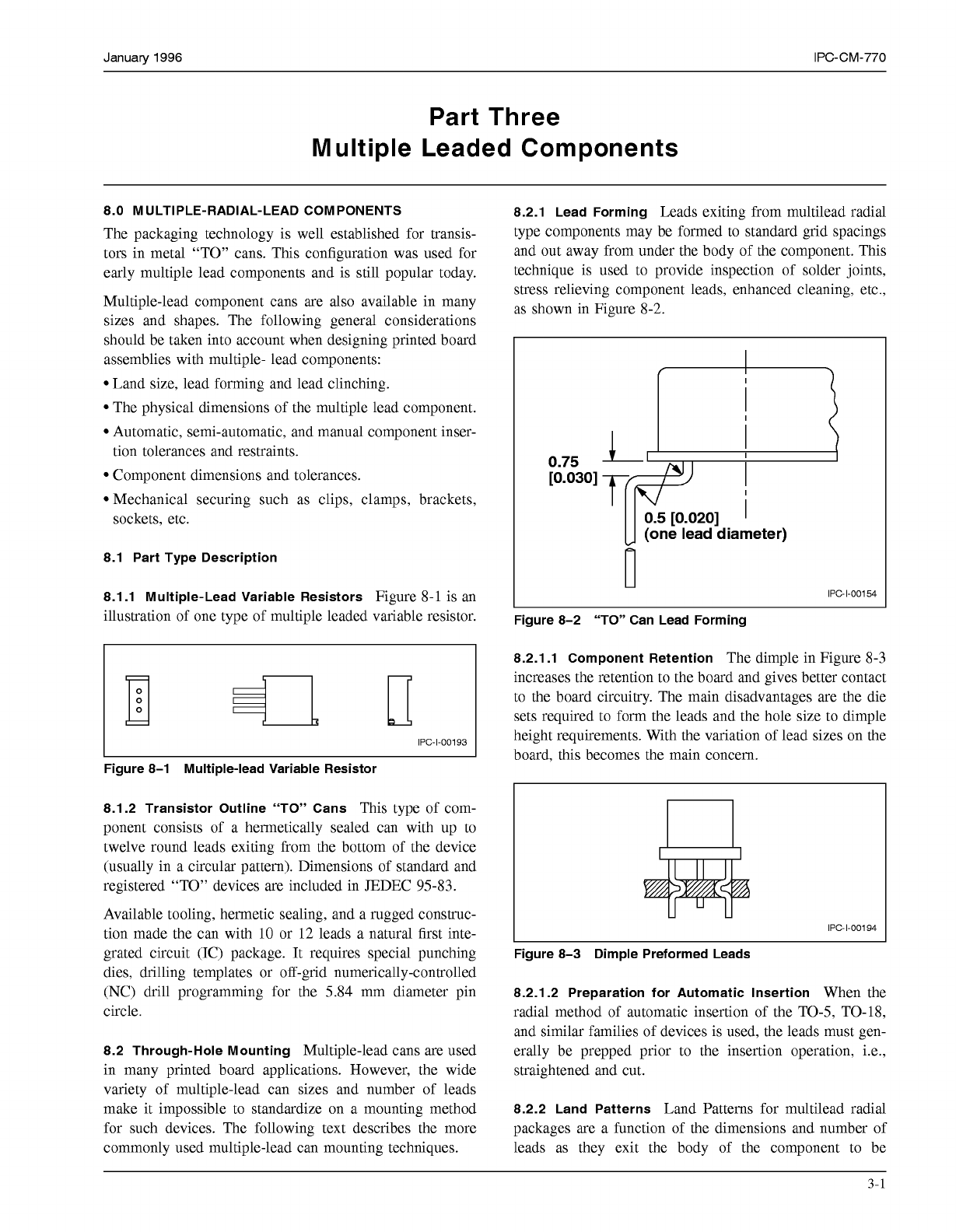
8.1.1 Multiple-Lead Variable Resistors
Figure 8-1 is an
illustration of one type of multiple leaded variable resistor.
IPC-1-00193
Figure 8-1 Multiple-lead Variable Resistor
8.1.2 Transistor Outline “TO” Cans
This type of com-
ponent consists of a hermetically sealed can with up to
twelve round leads exiting from the bottom of the device
(usually in a circular pattern). Dimensions of standard and
registered “TO” devices are included in JEDEC 95-83.
Available tooling, hermetic sealing, and a rugged consmc-
tion made the can with
10
or 12 leads a natural first inte-
grated circuit (IC) package. It requires special punching
dies, drilling templates or off-grid numerically-controlled
(NC) drill programming for the 5.84 mm diameter pin
circle.
8.2 Through-Hole Mounting
Multiple-lead cans are used
in many printed board applications. However, the wide
variety of multiple-lead can sizes and number of leads
make it impossible to standardize on a mounting method
for such devices. The following text describes the more
commonly used multiple-lead can mounting techniques.
8.2.1 Lead Forming
Leads exiting from multilead radial
type components may be formed to standard grid spacings
and out away from under the body of the component. This
technique is used to provide inspection of solder joints,
stress relieving component leads, enhanced cleaning, etc.,
as shown in Figure 8-2.
0.75
yN--
T
II
0.5
[0.020]
I
(one lead diameter)
IPC-1-00154
Figure 8-2 “TO” Can Lead Forming
8.2.1.1 Component Retention
The dimple in Figure 8-3
increases the retention to the board and gives better contact
to the board circuitry. The main disadvantages are the die
sets required to form the leads and the hole size to dimple
height requirements. With the variation of lead sizes on the
board, this becomes the main concern.
IPC-1-00194
Figure 8-3 Dimple Preformed Leads
8.2.1.2 Preparation for Automatic Insertion
When the
radial method of automatic insertion of the TO-5, TO-18,
and similar families of devices is used, the leads must gen-
erally be prepped prior to the insertion operation, i.e.,
straightened and cut.
8.2.2 Land Patterns
Land Patterns for multilead radial
packages are a function of the dimensions and number of
leads as they exit the body of the component to be
3-1
COPYRIGHT Association Connecting Electronics Industries
Licensed by Information Handling Services
COPYRIGHT Association Connecting Electronics Industries
Licensed by Information Handling Services