IPC-CM-770D-1996 - 第39页
January 1996 IPC-CM-770 Figure 8-7 Straight-through Lead, Unclinched Can IPC-1-00161 Figure 8-8 Offset Lead Can Mounting IPC-I-O0152 I L Figure 8-9 Transistor Mounting (Unsupported Holes) Where spacers or spreaders are u…
IPC-CM-770
Januaty
1996
mounted. Pattern configuration will also vary depending
upon the lead forming requirements as with spreader
mounting or reform into alternate patterns. Additional
information for hole/land requirements can be found in
Section 21.
In Figure 8-4, the leads of a TO-100 are formed to a stan-
dard 6.4 x 9.5 mm pattern, leaving space for two via or
plated holes available for internal plane connections or for
conductor routing. Lead forming provides a standoff and
protective coating is specified for the carrier surface to
insulate the printed wiring.
A typical printed board mounting pattern for 10-lead
multiple- lead cans with a 5.84 mm lead circle, such as
TO-96, TO-97, and TO-100, is shown in Figure 8-5.
O
O0
O0
ow0
O000
0000
Two Conductors
Per Channel
Lead Centers
3.18 [0.125]
All Conductors
0.33 [0.013]
All Spacing
0.25 [0.01 O]
Lands 1.65 [0.065]
Plated Hole 1
.O
[0.040]
Component Centers
12.7 [0.500]
Component Area
11.2 [0.400] dia.
IPC-1-00156
Figure 8-4 Typical TO-100 Can Layout (Inches Only)
The small lead circle dimensions require accurately located
lands, of a small diameter, with minimum annular rings.
8.2.3 Lead Configuration After Assembly
The basic
multiple- lead can mounting techniques can be grouped as
follows:
Straight-thru lead, unclinched
Straight-thru lead, clinched
Straight-thru lead, with spacer (clinched, unclinched or
swaged)
Preformed lead, unclinched
Preformed lead, clinched
Preformed lead, with spacer (clinched, unclinched, or
swaged)
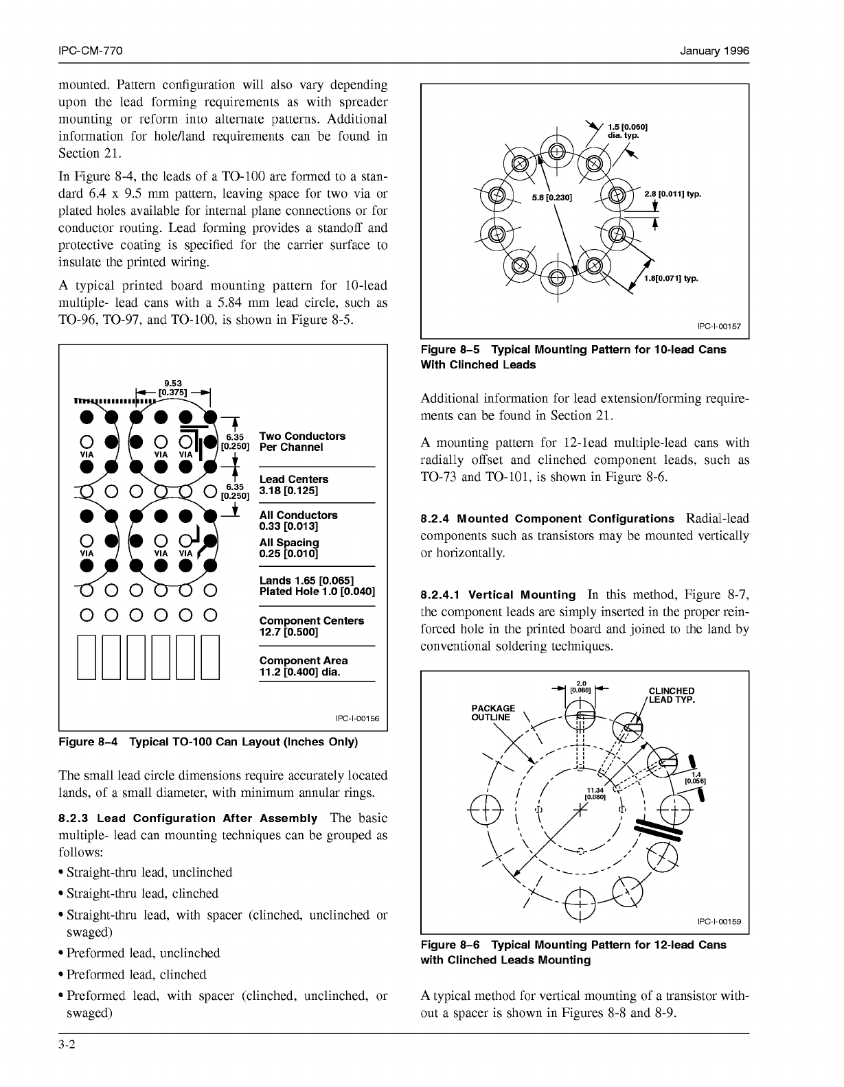
1.5
[0.060]
IPC-1-00157
Figure 8-5 Typical Mounting Pattern for 10-lead Cans
With Clinched Leads
Additional information for lead extension/forming require-
ments can be found in Section 21.
A mounting pattern for 12-lead multiple-lead cans with
radially offset and clinched component leads, such as
TO-73 and TO-101, is shown in Figure 8-6.
8.2.4 Mounted Component Configurations
Radial-lead
components such as transistors may be mounted vertically
or horizontally.
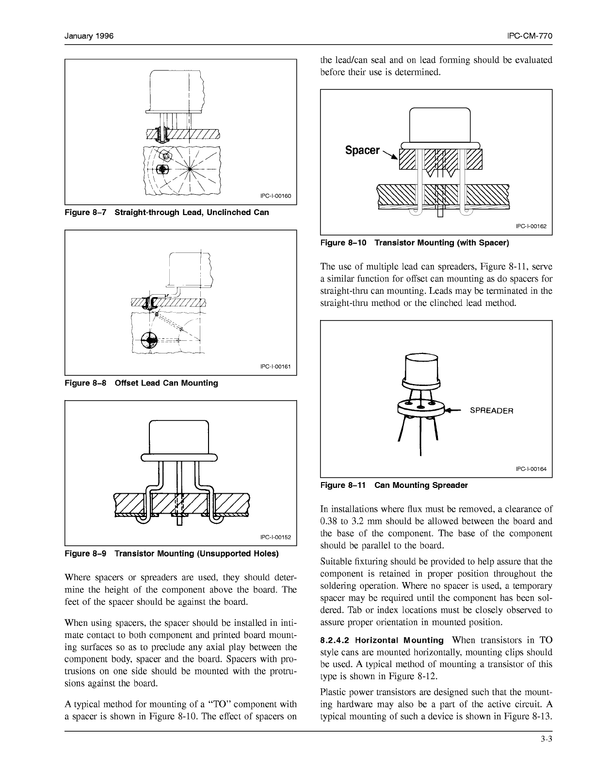
8.2.4.1 Vertical Mounting
In this method, Figure 8-7,
the component leads are simply inserted in the proper rein-
forced hole in the printed board and joined to the land by
conventional soldering techniques.
I
IPC-1-00159
Figure 8-6 Typical Mounting Pattern for 12-lead Cans
with Clinched Leads Mounting
A typical method for vertical mounting of a transistor with-
out a spacer is shown in Figures 8-8 and 8-9.
3-2
COPYRIGHT Association Connecting Electronics Industries
Licensed by Information Handling Services
COPYRIGHT Association Connecting Electronics Industries
Licensed by Information Handling Services
January
1996
IPC-CM-770
Figure 8-7 Straight-through Lead, Unclinched Can
IPC-1-00161
Figure 8-8 Offset Lead Can Mounting
IPC-I-O0152
I
L
Figure 8-9 Transistor Mounting (Unsupported Holes)
Where spacers or spreaders are used, they should deter-
mine the height of the component above the board. The
feet of the spacer should be against the board.
When using spacers, the spacer should be installed in inti-
mate contact to both component and printed board mount-
ing surfaces
so
as to preclude any axial play between the
component body, spacer and the board. Spacers with pro-
trusions on one side should be mounted with the protru-
sions against the board.
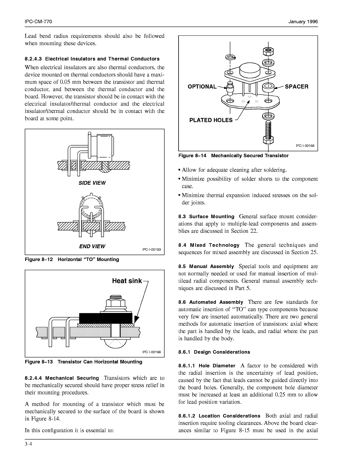
A
typical method for mounting of a “TO” component with
a spacer is shown in Figure 8-10. The effect of spacers on
the leadcan seal and on lead forming should be evaluated
before their use is determined.
Spacer
IPC-1-00162
Figure 8-10 Transistor Mounting (with Spacer)
The use of multiple lead can spreaders, Figure 8-11, serve
a similar function for offset can mounting as do spacers for
straight-thru can mounting. Leads may be terminated in the
straight-thru method or the clinched lead method.
SPREADER
IPC-1-00164
Figure 8-11 Can Mounting Spreader
In installations where flux must be removed, a clearance of
0.38 to 3.2 mm should be allowed between the board and
the base of the component. The base of the component
should be parallel to the board.
Suitable fixturing should be provided to help assure that the
component is retained in proper position throughout the
soldering operation. Where no spacer is used, a temporary
spacer may be required until the component has been sol-
dered. Tab or index locations must be closely observed to
assure proper orientation in mounted position.
8.2.4.2 Horizontal Mounting
When transistors in TO
style cans are mounted horizontally, mounting clips should
be used.
A
typical method of mounting a transistor of this
type is shown in Figure 8-12.
Plastic power transistors are designed such that the mount-
ing hardware may also be a part of the active circuit.
A
typical mounting of such a device is shown in Figure 8-13.
3-3
COPYRIGHT Association Connecting Electronics Industries
Licensed by Information Handling Services
COPYRIGHT Association Connecting Electronics Industries
Licensed by Information Handling Services
IPC-CM-770
Januaty
1996
Lead bend radius requirements should also be followed
when mounting these devices.
8.2.4.3 Electrical Insulators and Thermal Conductors
When electrical insulators are also thermal conductors, the
device mounted on thermal conductors should have a maxi-
mum space of
0.05
mm between the transistor and thermal
conductor, and between the thermal conductor and the
board. However, the transistor should be in contact with the
electrical insulator/thermal conductor and the electrical
insulator/thermal conductor should be in contact with the
board at some point.
SIDE VIEW
I
END VIEW
IPC-1-00153
I
OPTIONAL SPACER
Figure 8-14 Mechanically Secured Transistor
Allow for adequate cleaning after soldering.
Minimize possibility of solder shorts to the component
case.
Minimize thermal expansion induced stresses on the sol-
der joints.
8.3 Surface Mounting
General surface mount consider-
ations that apply to multiple-lead components and assem-
blies are discussed in Section
22.
8.4 Mixed Technology
The general techniques and
sequences for mixed assembly are discussed in Section
25.
Figure 8-1 2 Horizontal “TO” Mounting
8.5 Manual Assembly
Special tools and equipment are
not normally needed or used for manual insertion of mul-
tilead radial components. General manual assembly tech-
niques are discussed in Part
5.
U U
W
IPC-1-00166
I
8.6 Automated Assembly
There are few standards for
automatic insertion of “TO” can type components because
very few are inserted automatically. There are two general
methods for automatic insertion of transistors: axial where
the part is handled by the leads, and radial where the part
is handled by the body.
8.6.1 Design Considerations
Figure 8-1 3 Transistor Can Horizontal Mounting
8.2.4.4 Mechanical Securing
Transistors which are to
be mechanically secured should have proper stress relief in
their mounting procedures.
A method for mounting of a transistor which must be
mechanically secured to the surface of the board is shown
in Figure
8-14.
In this configuration it is essential to:
8.6.1.1 Hole Diameter
A factor to be considered with
the radial insertion is the uncertainty of lead position,
caused by the fact that leads cannot be guided directly into
the board holes. Generally, the component hole diameter
must be increased at least an additional
0.25
mm to allow
for lead position variation.
8.6.1.2 Location Considerations
Both axial and radial
insertion require tooling clearances. Above the board clear-
ances similar to Figure
8-15
must be used in the axial
3-4
COPYRIGHT Association Connecting Electronics Industries
Licensed by Information Handling Services
COPYRIGHT Association Connecting Electronics Industries
Licensed by Information Handling Services