IPC-CM-770D-1996 - 第43页
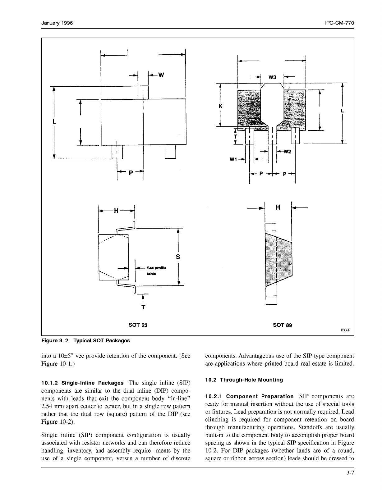
January 1996 IPC-CM-770 i I I l I I I L 'I t-"I t T SOT 23 t"i SOT 89 IPC-I- Typical SOT Packages into a 10+5" vee provide retention of the component. (See Figure 10- 1 .) 10.1.2 Single-lnline Package…
IPC-CM-770
Januaty
1996
view
+
7
4
040 150
tt
4
L-
o12
SO-16
(INCHES
SHOWN)
IPC-1.00375
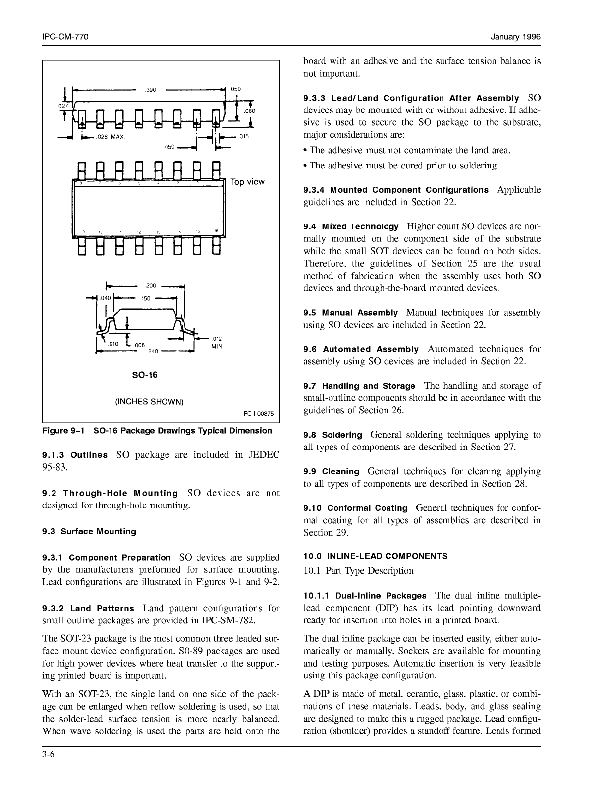
Figure 9-1 SO-1 6 Package Drawings Typical Dimension
9.1.3 Outlines
SO
package are included in JEDEC
95-83.
9.2 Through-Hole Mounting
so
devices are not
designed for through-hole mounting.
9.3 Surface Mounting
9.3.1 Component Preparation
SO
devices are supplied
by the manufacturers preformed for surface mounting.
Lead configurations are illustrated in Figures 9-1 and 9-2.
9.3.2 Land Patterns
Land pattern configurations for
small outline packages are provided in IPC-SM-782.
The SOT-23 package is the most common three leaded sur-
face mount device configuration. SO-89 packages are used
for high power devices where heat transfer to the support-
ing printed board is important.
With an SOT-23, the single land on one side of the pack-
age can be enlarged when reflow soldering is used,
so
that
the solder-lead surface tension is more nearly balanced.
When wave soldering is used the parts are held onto the
board with an adhesive and the surface tension balance is
not important.
9.3.3 LeadlLand Configuration After Assembly
so
devices may be mounted with or without adhesive.
If
adhe-
sive is used to secure the
SO
package to the substrate,
major considerations are:
The adhesive must not contaminate the land area.
The adhesive must be cured prior to soldering
9.3.4 Mounted Component Configurations
Applicable
guidelines are included in Section 22.
9.4 Mixed Technology
Higher count
SO
devices are nor-
mally mounted on the component side of the substrate
while the small SOT devices can be found on both sides.
Therefore, the guidelines of Section 25 are the usual
method of fabrication when the assembly uses both
SO
devices and through-the-board mounted devices.
9.5 Manual Assembly
Manual techniques for assembly
using
SO
devices are included in Section 22.
9.6 Automated Assembly
Automated techniques for
assembly using
SO
devices are included in Section 22.
9.7 Handling and Storage
The handling and storage of
small-outline components should be in accordance with the
guidelines of Section 26.
9.8 Soldering
General soldering techniques applying to
all types of components are described in Section 27.
9.9 Cleaning
General techniques for cleaning applying
to all types of components are described in Section 28.
9.1
O
Conformal Coating
General techniques for confor-
mal coating for all types of assemblies are described in
Section 29.
10.0 INLINE-LEAD COMPONENTS
10.1
Part Type Description
10.1.1 Dual-lnline Packages
The dual inline multiple-
lead component (DIP) has its lead pointing downward
ready for insertion into holes in a printed board.
The dual inline package can be inserted easily, either auto-
matically or manually. Sockets are available for mounting
and testing purposes. Automatic insertion is very feasible
using this package configuration.
A DIP is made of metal, ceramic, glass, plastic, or combi-
nations of these materials. Leads, body, and glass sealing
are designed to make this a rugged package. Lead configu-
ration (shoulder) provides a standoff feature. Leads formed
3-6
COPYRIGHT Association Connecting Electronics Industries
Licensed by Information Handling Services
COPYRIGHT Association Connecting Electronics Industries
Licensed by Information Handling Services
January
1996
IPC-CM-770
i
I
I
l
I
I
I
L
'I
t-"I
t
T
SOT
23
t"i
SOT
89
IPC-I-
Typical SOT Packages
into a
10+5"
vee provide retention of the component. (See
Figure
10-
1
.)
10.1.2 Single-lnline Packages
The single inline (SIP)
components are similar to the dual inline (DIP) compo-
nents with leads that exit the component body "in-line"
2.54
mm apart center to center, but in a single row pattern
rather that the dual row (square) pattern of the DIP (see
Figure
10-2).
Single inline (SIP) component configuration is usually
associated with resistor networks and can therefore reduce
handling, inventory, and assembly require- ments by the
use of a single component, versus a number of discrete
components. Advantageous use of the SIP type component
are applications where printed board real estate is limited.
10.2 Through-Hole Mounting
10.2.1 Component Preparation
SIP components are
ready for manual insertion without the use of special tools
or fixtures. Lead preparation is not normally required. Lead
clinching is required for component retention on board
through manufacturing operations. Standoffs are usually
built-in to the component body to accomplish proper board
spacing as shown in the typical SIP specification in Figure
10-2.
For DIP packages (whether lands are of a round,
square or ribbon across section) leads should be dressed to
3-7
COPYRIGHT Association Connecting Electronics Industries
Licensed by Information Handling Services
COPYRIGHT Association Connecting Electronics Industries
Licensed by Information Handling Services
IPC-CM-770
Januaty
1996
110.16
mm1
[.400"] max
2.54
mm
[.
1
OO"]
max
f
.25
mm
[.O1
O"]
non
accum
IPC-I-O0042
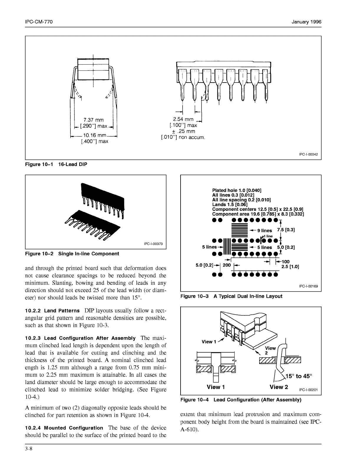
Figure 10-1 16-Lead DIP
IPC-1-00373
I
Figure 10-2 Single In-line Component
and through the printed board such that deformation does
not cause clearance spacings to be reduced beyond the
minimum. Slanting, bowing and bending of leads in any
direction should not exceed
25
of the lead width (or diam-
eter) nor should leads be twisted more than
15".
10.2.2 Land Patterns
DIP layouts usually follow a rect-
angular grid pattern and reasonable densities are possible,
such as that shown in Figure
10-3.
10.2.3 Lead Configuration After Assembly
The maxi-
mum clinched lead length is dependent upon the length of
lead that is available for cutting and clinching and the
thickness of the printed board.
A
nominal clinched lead
ength is
1.25
mm although a range from
0.75
mm mini-
mum to
2.25
mm maximum is attainable. In all cases the
land diameter should be large enough to accommodate the
clinched lead to minimize solder bridging. (See Figure
10-4.)
A
minimum of two
(2)
diagonally opposite leads should be
clinched for part retention as shown in Figure
10-4.
10.2.4 Mounted Configuration
The base of the device
should be parallel to the surface of the printed board to the
All
lines 0.3
[0.012]
Plated hole
1.0 [0.040]
All
line spacing 0.2 [0.010]
Lands 1.5 [0.06]
Component centers 12.5 [0.5]
x
22.5 [0.9]
Component area 19.6 [0.785]
x
8.3 [0.332]
0.
........
f
-
-
9 lines 7.5 10.31
5
lin es^^^^^^
-5 lines 5.0 [0.2]
0.
........*
5.0 [0.2]--1 200
"I
IPC-1-00169
Figure 10-3 A Typical Dual In-line Layout
View 1
d
I
View
1
View
IPC-I-O0201
Figure 10-4 Lead Configuration (After Assembly)
extent that minimum lead protrusion and maximum com-
ponent body height from the board is maintained (see IPC-
A-610).
3-8
COPYRIGHT Association Connecting Electronics Industries
Licensed by Information Handling Services
COPYRIGHT Association Connecting Electronics Industries
Licensed by Information Handling Services