IPC-CM-770D-1996 - 第46页
IPC-CM-770 Januaty 1996 contact with the solder paste or tin/lead plating being reflowed. Proper handling is required so that components do not move prior to the reflow soldering operation. í - - I- o- I’ IPC-I-O0270 Fig…
January
1996
IPC-CM-770
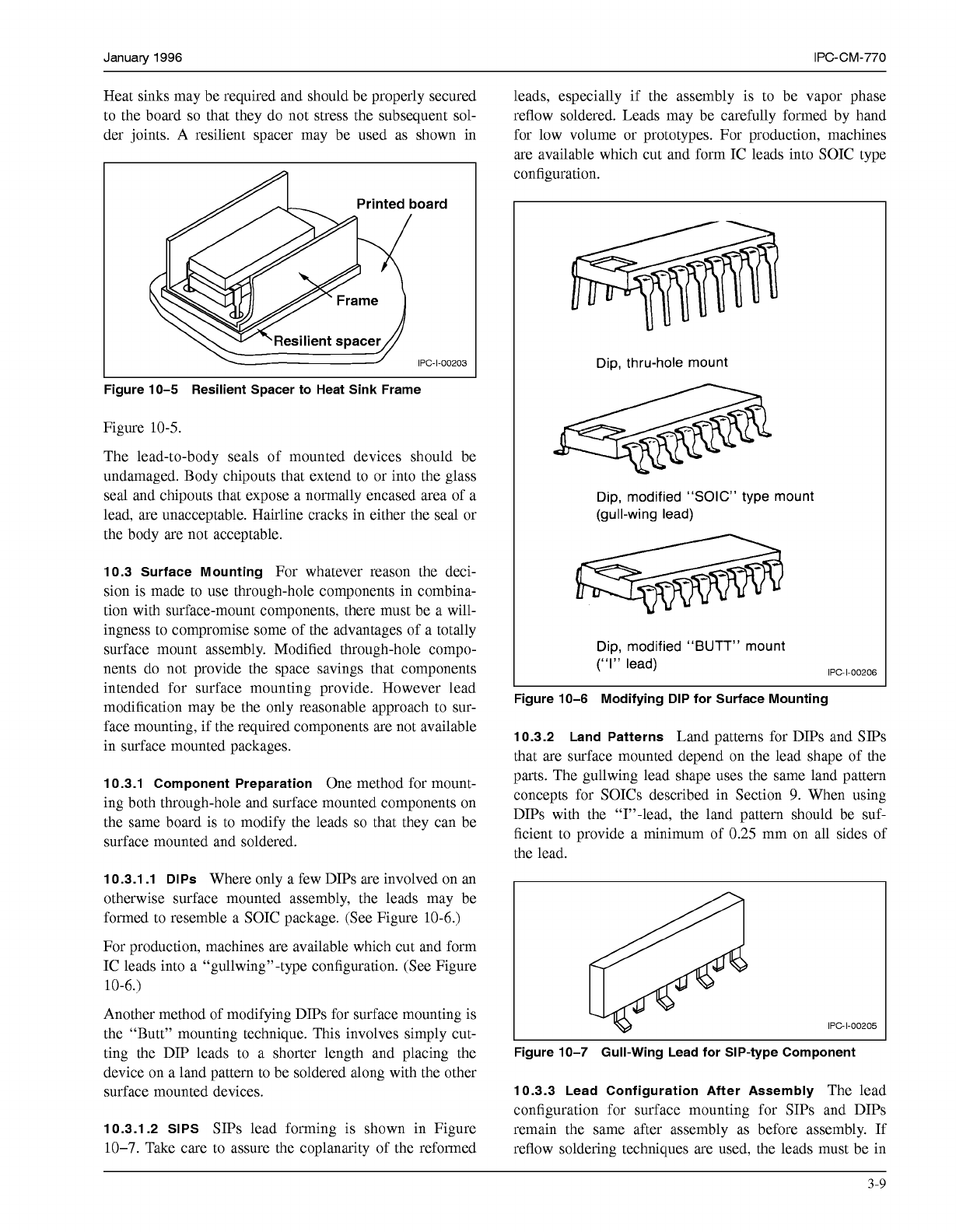
Heat sinks may be required and should be properly secured
to the board
so
that they do not stress the subsequent sol-
der joints. A resilient spacer may be used as shown in
\\V
“Resilient spacer
//
\
1
IPC-I-O0203
I
L
Figure 10-5 Resilient Spacer to Heat Sink Frame
Figure
10-5.
The lead-to-body seals of mounted devices should be
undamaged. Body chipouts that extend to or into the glass
seal and chipouts that expose a normally encased area of a
lead, are unacceptable. Hairline cracks in either the seal or
the body are not acceptable.
10.3 Surface Mounting
For whatever reason the deci-
sion is made to use through-hole components in combina-
tion with surface-mount components, there must be a will-
ingness to compromise some of the advantages of a totally
surface mount assembly. Modified through-hole compo-
nents do not provide the space savings that components
intended for surface mounting provide. However lead
modification may be the only reasonable approach to sur-
face mounting, if the required components are not available
in surface mounted packages.
10.3.1 Component Preparation
One method for mount-
ing both through-hole and surface mounted components on
the same board is to modify the leads
so
that they can be
surface mounted and soldered.
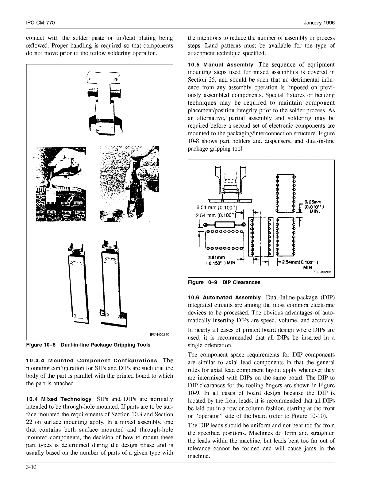
10.3.1.1 DIPS
Where only a few DIPs are involved on an
otherwise surface mounted assembly, the leads may be
formed to resemble a SOIC package. (See Figure
10-6.)
For production, machines are available which cut and form
IC leads into a “gullwing”-type configuration. (See Figure
10-6.)
Another method of modifying DIPs for surface mounting is
the “Butt” mounting technique. This involves simply cut-
ting the DIP leads to a shorter length and placing the
device on a land pattern to be soldered along with the other
surface mounted devices.
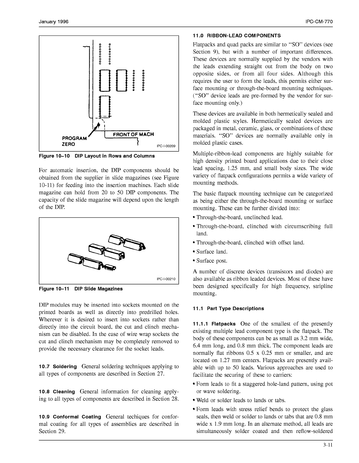
10.3.1.2 SIPS
SIPs lead forming is shown in Figure
10-7.
Take care to assure the coplanarity of the reformed
leads, especially if the assembly is to be vapor phase
reflow soldered. Leads may be carefully formed by hand
for low volume or prototypes. For production, machines
are available which cut and form IC leads into SOIC type
configuration.
Dip, thru-hole mount
Dip, modified
“SOIC”
type mount
(gull-wing lead)
Dip, modified
“BUTT”
mount
(“I”
lead)
IPC-I-O0206
Figure 10-6 Modifying DIP for Surface Mounting
10.3.2 Land Patterns
Land patterns for DIPs and
SIPs
that are surface mounted depend on the lead shape of the
parts. The gullwing lead shape uses the same land pattern
concepts for SOICs described in Section
9.
When using
DIPs with the “1”-lead, the land pattern should be suf-
ficient to provide a minimum of
0.25
mm on all sides of
the lead.
Figure 10-7 Gull-Wing Lead for SIP-type Component
10.3.3 Lead Configuration After Assembly
The lead
configuration for surface mounting for SIPs and DIPs
remain the same after assembly as before assembly. If
reflow soldering techniques are used, the leads must be in
3-9
COPYRIGHT Association Connecting Electronics Industries
Licensed by Information Handling Services
COPYRIGHT Association Connecting Electronics Industries
Licensed by Information Handling Services
IPC-CM-770
Januaty
1996
contact with the solder paste or tin/lead plating being
reflowed. Proper handling is required
so
that components
do not move prior to the reflow soldering operation.
í
-
-
I-
o-
I’
IPC-I-O0270
Figure 10-8 Dual-in-line Package Gripping Tools
10.3.4 Mounted Component Configurations
The
mounting configuration for SIPS and DIPs are such that the
body of the part is parallel with the printed board to which
the part is attached.
10.4 Mixed Technology
SIPS and DIPS are normally
intended to be through-hole mounted. If parts are to be sur-
face mounted the requirements of Section
10.3
and Section
22
on surface mounting apply. In a mixed assembly, one
that contains both surface mounted and through-hole
mounted components, the decision of how to mount these
part types is determined during the design phase and is
usually based on the number of parts of a given type with
the intentions to reduce the number of assembly or process
steps. Land patterns must be available for the type of
attachment technique specified.
10.5 Manual Assembly
The sequence of equipment
mounting steps used for mixed assemblies is covered in
Section
25,
and should be such that no detrimental influ-
ence from any assembly operation is imposed on previ-
ously assembled components. Special fixtures or bending
techniques may be required to maintain component
placemendposition integrity prior to the solder process.
As
an alternative, partial assembly and soldering may be
required before a second set of electronic components are
mounted to the
packaging/interconnection
structure. Figure
10-8
shows part holders and dispensers, and dual-in-line
package gripping tool.
I
IPC-I-O0208
Figure 10-9 DIP Clearances
10.6 Automated Assembly
Dual-Inline-package (DIP)
integrated circuits are among the most common electronic
devices to be processed. The obvious advantages of auto-
matically inserting DIPs are speed, volume, and accuracy.
In nearly all cases of printed board design where DIPs are
used, it is recommended that all DIPs be inserted in a
single orientation.
The component space requirements for DIP components
are similar to axial lead components in that the general
rules for axial lead component layout apply whenever they
are intermixed with DIPs on the same board. The DIP to
DIP clearances for the tooling fingers are shown in Figure
10-9.
In all cases of board design because the DIP is
located by the front leads, it is recommended that all DIPs
be laid out in a row or column fashion, starting at the front
or “operator” side of the board (refer to Figure
10-10).
The DIP leads should be uniform and not bent too far from
the specified positions. Machines do form and straighten
the leads within the machine, but leads bent too
far
out of
tolerance cannot be formed and will cause jams in the
machine.
3-10
COPYRIGHT Association Connecting Electronics Industries
Licensed by Information Handling Services
COPYRIGHT Association Connecting Electronics Industries
Licensed by Information Handling Services
January
1996
IPC-CM-770
PROGRAM
ZERO
IPC-I-O0209
I
Figure
10-10
DIP Layout in
Rows
and Columns
For automatic insertion, the DIP components should be
obtained from the supplier in slide magazines (see Figure
10-11)
for feeding into the insertion machines. Each slide
magazine can hold from 20 to
50
DIP components. The
capacity of the slide magazine will depend upon the length
of the DIP.
IPC-I-O0210
I
L
Figure
10-11
DIP Slide Magazines
DIP modules may be inserted into sockets mounted on the
printed boards as well as directly into predrilled holes.
Wherever it is desired to insert into sockets rather than
directly into the circuit board, the cut and clinch mecha-
nism can be disabled. In the case of wire wrap sockets the
cut and clinch mechanism may be completely removed to
provide the necessary clearance for the socket leads.
10.7
Soldering
General soldering techniques applying to
all types of components are described in Section 27.
10.8
Cleaning
General information for cleaning apply-
ing to all types of components are described in Section 28.
10.9
Conformal Coating
General techiques for confor-
mal coating for all types of assemblies are described in
Section 29.
11
.O
RIBBON-LEAD COMPONENTS
Flatpacks and quad packs are similar to
“SO”
devices (see
Section 9), but with a number of important differences.
These devices are normally supplied by the vendors with
the leads extending straight out from the body on two
opposite sides, or from all four sides. Although this
requires the user to form the leads, this permits either sur-
face mounting or through-the-board mounting techniques.
(“SO”
device leads are pre-formed by the vendor for sur-
face mounting only.)
These devices are available in both hermetically sealed and
molded plastic styles. Hermetically sealed devices are
packaged in metal, ceramic, glass, or combinations of these
materials.
“SO”
devices are normally available only in
molded plastic cases.
Multiple-ribbon-lead components are highly suitable for
high density printed board applications due to their close
lead spacing, 1.25 mm, and small body sizes. The wide
variety of flatpack configurations permits a wide variety of
mounting methods.
The basic flatpack mounting technique can be categorized
as being either the through-the-board mounting or surface
mounting. These can be further divided into:
Through-the-board, unclinched lead.
Through-the-board, clinched with circumscribing full
land.
Through-the-board, clinched with offset land.
Surface land.
Surface post.
A number of discrete devices (transistors and diodes) are
also available as ribbon leaded devices. Most of these have
been designed specifically for high frequency, stripline
mounting.
11.1 Part Type Descriptions
11.1.1 Flatpacks
One of the smallest of the presently
existing multiple lead component type is the flatpack. The
body of these components can be as small as 3.2 mm wide,
6.4
mm long, and 0.8 mm thick. The component leads are
normally flat ribbons
0.5
x 0.25 mm or smaller, and are
located on 1.27 mm centers. Flatpacks are presently avail-
able with up to
50
leads. Various approaches are used to
facilitate the securing of these to carriers:
Form leads to fit a staggered hole-land pattern, using pot
or wave soldering.
Weld or solder leads to lands or tabs.
Form leads with stress relief bends to protect the glass
seals, then weld or solder to lands or tabs that are 0.8 mm
wide x 1.9 mm long. In an alternate method, all leads are
simultaneously solder coated and then reflow-soldered
3-11
COPYRIGHT Association Connecting Electronics Industries
Licensed by Information Handling Services
COPYRIGHT Association Connecting Electronics Industries
Licensed by Information Handling Services