IPC-CM-770D-1996 - 第49页
January 1996 IPC-CM-770 -” IPC-I-O0213 2t but not less than L Mar - Maxlrnurn Body length or wldth (including extensions such as lead fillets (both sides), glass seals, etc.] W - Nominal lead mdth t - Nominal lead lhlckn…
IPC-CM-770
Januaty
1996
with semiautomatic insertion equipment.
Flatpacks must be insulated when placed over conductive
traces. Unless the user has control over the particular pack-
age material, it may be appropriate to provide insulation
between the bottom of the flatpack and any conductive
traces, regardless of the case material being used.
Users of flatpacks have had problems from non-standard
shipping containers. Another flatpack problem is that the
automated assembly cost is very high compared to other
packages, owing to the fragile leads and the special care
required in assembly.
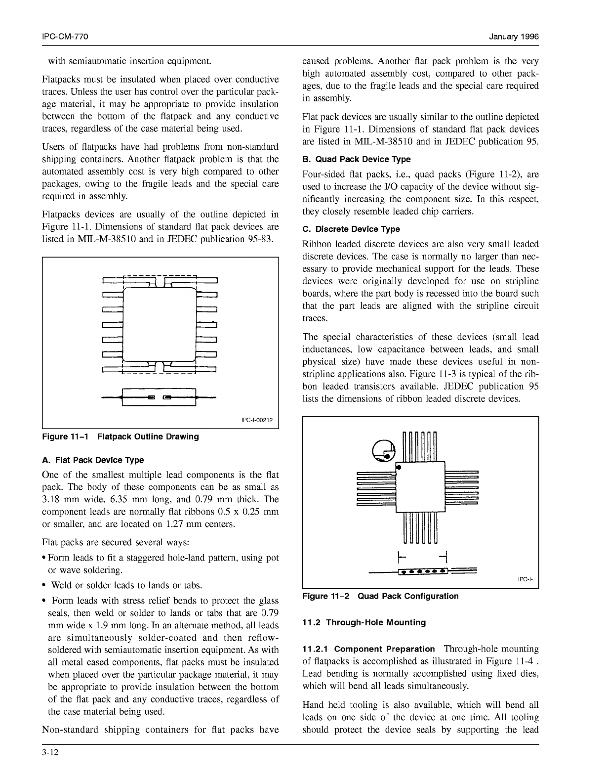
Flatpacks devices are usually of the outline depicted in
Figure
11-1.
Dimensions of standard flat pack devices are
listed in MIL-M-38510 and in JEDEC publication 95-83.
E
IPC-I-O0212
Figure 11-1 Flatpack Outline Drawing
A.
Flat Pack Device Type
One of the smallest multiple lead components is the flat
pack. The body of these components can be as small as
3.18 mm wide, 6.35 mm long, and 0.79 mm thick. The
component leads are normally flat ribbons
0.5
x 0.25 mm
or smaller, and are located on 1.27 mm centers.
Flat packs are secured several ways:
Form leads to fit a staggered hole-land pattern, using pot
or wave soldering.
Weld or solder leads to lands or tabs.
Form leads with stress relief bends to protect the glass
seals, then weld or solder to lands or tabs that are 0.79
mm wide x 1.9 mm long. In an alternate method, all leads
are simultaneously solder-coated and then reflow-
soldered with semiautomatic insertion equipment. As with
all metal cased components, flat packs must be insulated
when placed over the particular package material, it may
be appropriate to provide insulation between the bottom
of the flat pack and any conductive traces, regardless
of
the case material being used.
Non-standard shipping containers for flat packs have
caused problems. Another flat pack problem is the very
high automated assembly cost, compared to other pack-
ages, due to the fragile leads and the special care required
in assembly.
Flat pack devices are usually similar to the outline depicted
in Figure
11-1.
Dimensions of standard flat pack devices
are listed in MIL-M-38510 and in JEDEC publication 95.
B.
Quad Pack Device Type
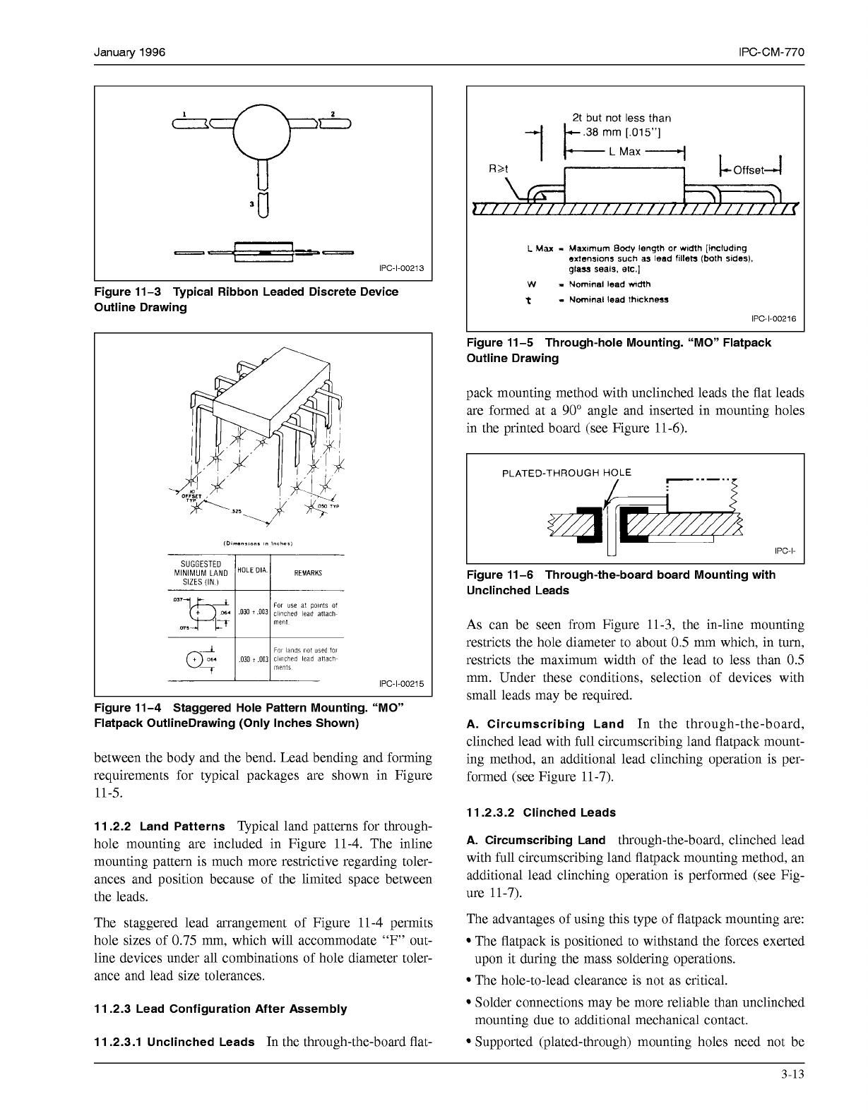
Four-sided flat packs, i.e., quad packs (Figure 11-2), are
used to increase the
Il0
capacity of the device without sig-
nificantly increasing the component size. In this respect,
they closely resemble leaded chip carriers.
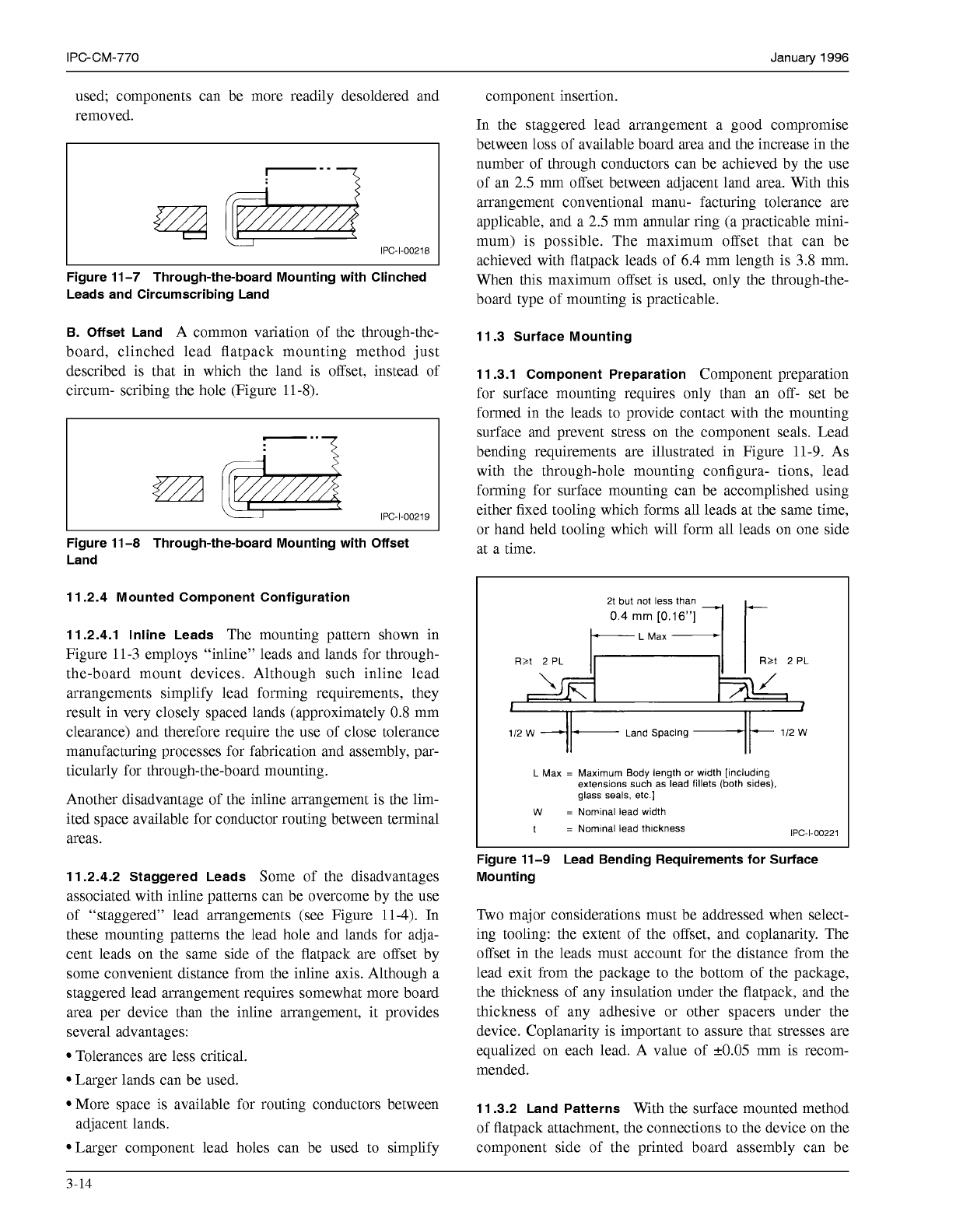
C. Discrete Device Type
Ribbon leaded discrete devices are also very small leaded
discrete devices. The case is normally no larger than nec-
essary to provide mechanical support for the leads. These
devices were originally developed for use on stripline
boards, where the part body is recessed into the board such
that the part leads are aligned with the stripline circuit
traces.
The special characteristics of these devices (small lead
inductances, low capacitance between leads, and small
physical size) have made these devices useful in non-
stripline applications also. Figure 11-3 is typical of the rib-
bon leaded transistors available. JEDEC publication 95
lists the dimensions of ribbon leaded discrete devices.
t-
-1
Figure 11-2 Quad Pack Configuration
11.2 Through-Hole Mounting
11 2.1 Component Preparation
Through-hole mounting
of flatpacks is accomplished as illustrated in Figure
11-4
.
Lead bending is normally accomplished using fixed dies,
which will bend all leads simultaneously.
Hand held tooling is also available, which will bend all
leads on one side of the device at one time. All tooling
should protect the device seals by supporting the lead
3-12
COPYRIGHT Association Connecting Electronics Industries
Licensed by Information Handling Services
COPYRIGHT Association Connecting Electronics Industries
Licensed by Information Handling Services
January
1996
IPC-CM-770
-”
IPC-I-O0213
2t
but
not
less
than
L
Mar
-
Maxlrnurn
Body
length
or
wldth (including
extensions
such
as
lead fillets (both sides),
glass
seals,
etc.]
W
-
Nominal lead mdth
t
-
Nominal lead lhlcknew
I
IPC-1-00216
Figure 11-3 Typical Ribbon Leaded Discrete Device
Outline Drawing
Figure 11-5 Through-hole Mounting. “MO” Flatpack
Outline Drawing
pack mounting method with unclinched leads the flat leads
are formed at a
90”
angle and inserted in mounting holes
in the printed board (see Figure
11-6).
SUGGESTED
SIZES
(IN
i
I
I
Figure 11-4 Staggered Hole Pattern Mounting. “MO”
Flatpack OutlineDrawing (Only Inches Shown)
between the body and the bend. Lead bending and forming
requirements for typical packages are shown in Figure
11-5.
11.2.2 Land Patterns
Typical land patterns for through-
hole mounting are included in Figure
11-4.
The inline
mounting pattern is much more restrictive regarding toler-
ances and position because of the limited space between
the leads.
The staggered lead arrangement of Figure
11-4
permits
hole sizes of
0.75
mm, which will accommodate
“F”
out-
line devices under all combinations of hole diameter toler-
ance and lead size tolerances.
11.2.3 Lead Configuration After Assembly
11.2.3.1 Unclinched Leads
In the through-the-board flat-
PLATED-THROUGH
HOLE
/
Figure 11-6 Through-the-board board Mounting with
Unclinched Leads
As
can be seen from Figure
11-3,
the in-line mounting
restricts the hole diameter to about
0.5
mm which, in turn,
restricts the maximum width of the lead to less than
0.5
mm. Under these conditions, selection of devices with
small leads may be required.
A. Circumscribing Land
In the through-the-board,
clinched lead with full circumscribing land flatpack mount-
ing method, an additional lead clinching operation is per-
formed (see Figure
11-7).
11.2.3.2 Clinched Leads
A. Circumscribing Land
through-the-board, clinched lead
with full circumscribing land flatpack mounting method, an
additional lead clinching operation is performed (see Fig-
ure
11-7).
The advantages of using this type of flatpack mounting are:
The flatpack is positioned to withstand the forces exerted
upon it during the mass soldering operations.
The hole-to-lead clearance is not as critical.
Solder connections may be more reliable than unclinched
mounting due to additional mechanical contact.
Supported (plated-through) mounting holes need not be
3-13
COPYRIGHT Association Connecting Electronics Industries
Licensed by Information Handling Services
COPYRIGHT Association Connecting Electronics Industries
Licensed by Information Handling Services
IPC-CM-770
Januaty
1996
used; components can be more readily desoldered and
removed.
a
IPC-I-O0218
Figure 11-7 Through-the-board Mounting with Clinched
Leads and Circumscribing Land
B. Offset Land
A common variation of the through-the-
board, clinched lead flatpack mounting method just
described is that in which the land is offset, instead of
circum- scribing the hole (Figure 11-8).
IPC-I-O0219
Figure 11-8 Through-the-board Mounting with Offset
Land
11.2.4 Mounted Component Configuration
11.2.4.1 lnline Leads
The mounting pattern shown in
Figure 11-3 employs “inline” leads and lands for through-
the-board mount devices. Although such inline lead
arrangements simplify lead forming requirements, they
result in very closely spaced lands (approximately 0.8 mm
clearance) and therefore require the use of close tolerance
manufacturing processes for fabrication and assembly, par-
ticularly for through-the-board mounting.
Another disadvantage of the inline arrangement is the lim-
ited space available for conductor routing between terminal
areas.
11.2.4.2 Staggered Leads
Some of the disadvantages
associated with inline patterns can be overcome by the use
of “staggered” lead arrangements (see Figure
11-4).
In
these mounting patterns the lead hole and lands for adja-
cent leads on the same side of the flatpack are offset by
some convenient distance from the inline axis. Although a
staggered lead arrangement requires somewhat more board
area per device than the inline arrangement, it provides
several advantages:
Tolerances are less critical.
Larger lands can be used.
More space is available for routing conductors between
adjacent lands.
Larger component lead holes can be used to simplify
component insertion.
In the staggered lead arrangement a good compromise
between loss of available board area and the increase in the
number of through conductors can be achieved by the use
of an
2.5
mm offset between adjacent land area. With this
arrangement conventional manu- facturing tolerance are
applicable, and a
2.5
mm annular ring (a practicable mini-
mum) is possible. The maximum offset that can be
achieved with flatpack leads of
6.4
mm length is 3.8 mm.
When this maximum offset is used, only the through-the-
board type of mounting is practicable.
11.3 Surface Mounting
11.3.1 Component Preparation
Component preparation
for surface mounting requires only than an off- set be
formed in the leads to provide contact with the mounting
surface and prevent stress on the component seals. Lead
bending requirements are illustrated in Figure
11-9.
As
with the through-hole mounting configura- tions, lead
forming for surface mounting can be accomplished using
either fixed tooling which forms all leads at the same time,
or hand held tooling which will form all leads on one side
at a time.
21
but
not
less
than
0.4
mm
[0.16”]
7
I
I
112
W
-
-
1/2
W
Land Spacing
+
L
Max
=
Maxlmurn Body length
or
wldth [includmg
extensions such as lead fillets (both sides),
glass seals, etc
]
W
=
Normnal lead width
t
=
NomInal lead thickness
IPC-I-O0221
Figure 11-9 Lead Bending Requirements for Surface
Mounting
Two major considerations must be addressed when select-
ing tooling: the extent of the offset, and coplanarity. The
offset in the leads must account for the distance from the
lead exit from the package to the bottom of the package,
the thickness of any insulation under the flatpack, and the
thickness of any adhesive or other spacers under the
device. Coplanarity is important to assure that stresses are
equalized on each lead. A value of
k0.05
mm is recom-
mended.
11.3.2 Land Patterns
With the surface mounted method
of flatpack attachment, the connections to the device on the
component side of the printed board assembly can be
3-14
COPYRIGHT Association Connecting Electronics Industries
Licensed by Information Handling Services
COPYRIGHT Association Connecting Electronics Industries
Licensed by Information Handling Services