IPC-CM-770D-1996 - 第52页
IPC-CM-770 Januaty 1996 Lead extends beyond edge of land greater than 0.12 mm [.005”] NOT RECOMMENDED IPC-I-O0058 Figure 11 -1 4 Lead Extension (a) “Post” Method (b) “Surface Land” Method IPC-I- Figure 11-15 Welded Confi…
January
1996
IPC-CM-770
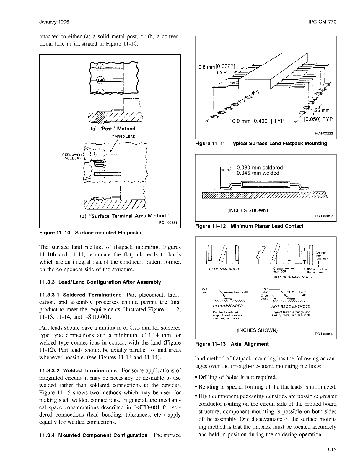
attached to either (a) a solid metal post, or
(b)
a conven-
tional land as illustrated in Figure
11-10.
(a)
"Post" Method
TINNED
LEAD
(b)
"Surface
Terminal Area
Method"
IPC-1-00381
Figure 11-10 Surface-mounted Flatpacks
The surface land method of flatpack mounting, Figures
11-10b and
11-11,
terminate the flatpack leads to lands
which are an integral part of the conductor pattern formed
on the component side of the structure.
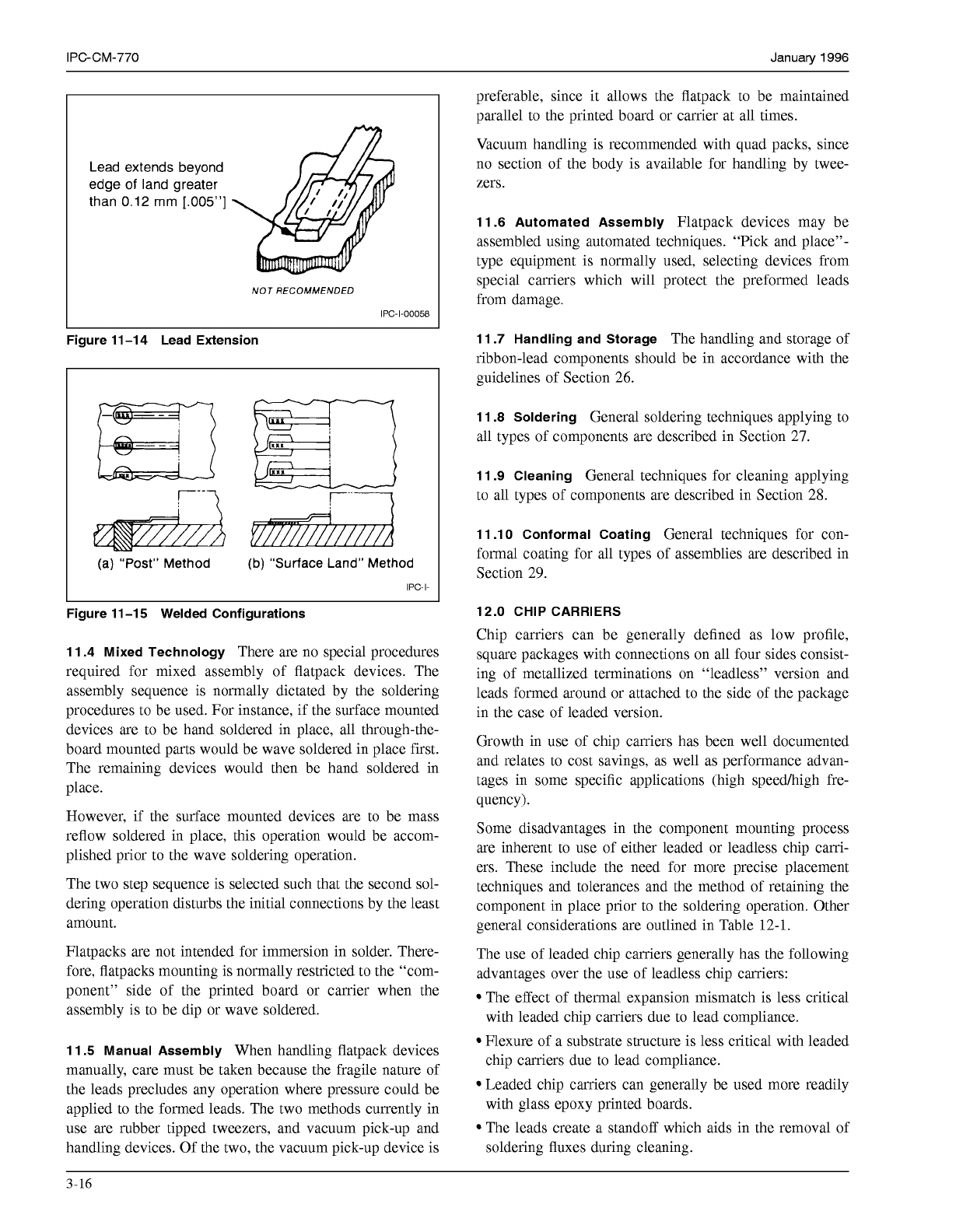
11.3.3 LeadlLand Configuration After Assembly
11.3.3.1 Soldered Terminations
Part placement, fabri-
cation, and assembly processes should permit the final
product to meet the requirements illustrated Figure
11-12,
11-13,
11-14,
and J-STD-001.
Part leads should have a minimum of
0.75
mm for soldered
type type connections and a minimum of
1.14
mm for
welded type connections in contact with the land (Figure
11-12).
Part leads should be axially parallel to land areas
whenever possible. (see Figures
11-13
and
11-14).
11.3.3.2 Welded Terminations
For some applications of
integrated circuits it may be necessary or desirable to use
welded rather than soldered connections to the devices.
Figure
11-15
shows two methods which may be used for
making such welded connections. In general, the mechani-
cal space considerations described in J-STD-O01 for sol-
dered connections (lead bending, tolerances, etc.) apply
equally for welded connections.
11.3.4 Mounted Component Configuration
The surface
I
IPC-I-O0222
Figure 11-11 Typical Surface Land Flatpack Mounting
0.030
rnin
soldered
0.045
rnin
welded
(INCHES SHOWN)
IPC-1-00057
Figure 11-12 Minimum Planar Lead Contact
RECOMMENDED
L
030
mlnlsolder
045
mln
weld
NOT
RECOMMENDED
I
RECOMMENDED NOT RECOMMENDED
Pan lead centered
or
edge
of
lead
does not
Edge
of
lead overhangs land
overhang land
area
area
by
more
than
005 Inch
(INCHES SHOWN)
IPC-1-00056
Figure 11-13 Axial Alignment
land method of flatpack mounting has the following advan-
tages over the through-the-board mounting methods:
Drilling of holes is not required.
Bending or special forming of the flat leads is minimized.
High component packaging densities are possible; greater
conductor routing on the circuit side of the printed board
structure; component mounting is possible on both sides
of the assembly. One disadvantage of the surface mount-
ing method is that the flatpack must be located accurately
and held in position during the soldering operation.
3-15
COPYRIGHT Association Connecting Electronics Industries
Licensed by Information Handling Services
COPYRIGHT Association Connecting Electronics Industries
Licensed by Information Handling Services
IPC-CM-770
Januaty
1996
Lead extends beyond
edge
of
land greater
than
0.12
mm
[.005”]
NOT
RECOMMENDED
IPC-I-O0058
Figure 11 -1 4 Lead Extension
(a)
“Post”
Method
(b)
“Surface Land” Method
IPC-I-
Figure 11-15 Welded Configurations
1 1.4 Mixed Technology
There are no special procedures
required for mixed assembly of flatpack devices. The
assembly sequence is normally dictated by the soldering
procedures to be used. For instance, if the surface mounted
devices are to be hand soldered in place, all through-the-
board mounted parts would be wave soldered in place first.
The remaining devices would then be hand soldered in
place.
However, if the surface mounted devices are to be mass
reflow soldered in place, this operation would be accom-
plished prior to the wave soldering operation.
The two step sequence is selected such that the second sol-
dering operation disturbs the initial connections by the least
amount.
Flatpacks are not intended for immersion in solder. There-
fore, flatpacks mounting is normally restricted to the “com-
ponent” side of the printed board or carrier when the
assembly is to be dip or wave soldered.
11.5 Manual Assembly
When handling flatpack devices
manually, care must be taken because the fragile nature of
the leads precludes any operation where pressure could be
applied to the formed leads. The two methods currently in
use are rubber tipped tweezers, and vacuum pick-up and
handling devices. Of the two, the vacuum pick-up device is
preferable, since it allows the flatpack to be maintained
parallel to the printed board or carrier at all times.
Vacuum handling is recommended with quad packs, since
no section of the body is available for handling by twee-
zers.
11.6 Automated Assembly
Flatpack devices may be
assembled using automated techniques. “Pick and place”-
type equipment is normally used, selecting devices from
special carriers which will protect the preformed leads
from damage.
11.7 Handling and Storage
The handling and storage of
ribbon-lead components should be in accordance with the
guidelines of Section
26.
11.8 Soldering
General soldering techniques applying to
all types of components are described in Section
27.
11.9 Cleaning
General techniques for cleaning applying
to all types of components are described in Section
28.
11.1
O
Conformal Coating
General techniques for con-
formal coating for all types of assemblies are described in
Section
29.
12.0 CHIP CARRIERS
Chip carriers can be generally defined as low profile,
square packages with connections on all four sides consist-
ing of metallized terminations on “leadless” version and
leads formed around or attached to the side of the package
in the case of leaded version.
Growth in use of chip carriers has been well documented
and relates to cost savings, as well as performance advan-
tages in some specific applications (high speedhigh fre-
quency).
Some disadvantages in the component mounting process
are inherent to use of either leaded or leadless chip carri-
ers. These include the need for more precise placement
techniques and tolerances and the method of retaining the
component in place prior to the soldering operation. Other
general considerations are outlined in Table
12-1.
The use of leaded chip carriers generally has the following
advantages over the use of leadless chip carriers:
The effect of thermal expansion mismatch is less critical
with leaded chip carriers due to lead compliance.
Flexure of a substrate structure is less critical with leaded
chip carriers due to lead compliance.
Leaded chip carriers can generally be used more readily
with glass epoxy printed boards.
The leads create a standoff which aids in the removal of
soldering fluxes during cleaning.
3-16
COPYRIGHT Association Connecting Electronics Industries
Licensed by Information Handling Services
COPYRIGHT Association Connecting Electronics Industries
Licensed by Information Handling Services
January
1996
IPC-CM-770
The use of leaded chip carriers generally has the following carriers have a chamfered index comer that is larger than
disadvantages when compared to the use of leadless chip that of type C. Another difference between the A,
B
and D
carriers: types and type C is the feature in the other three comers
When used, the application of clip leads requires addi-
(see Figure 12-21. The types A,
B
and D were designed for
tional
process
and inspection steps, thereby increasing socket applications and printed wiring interconnections.
through reflow soldering. This application difference is the
main reason for their mechanical differences. All have
compatible terminal locations. These packages mount in
costs. The type C is primarily intended for direct attachment
The length of leaded chip carrier terminals may signifi-
cantly increase lead inductance.
The leaded chip MtTier package does not have as direct a different orientations, depending on type, mounting
strut-
path to conduction cooling through the substrate. ture and preferred thermal orientation.
Leads can be damaged in test and assembly.
Leadless type A is intended for lid-down mounting in a
Planarity of leads must be maintained for reliable solder socket, which places the primary heat-dissipating
surface
joints.
Table 12-1 Chip Carrier Application Considerations
Consideration Leaded CC Leadless CCs
Thermal expansion to match.
I
Critical.
I
Less critical.
I
Removal and replacement.
I
Comparatively easy with special tools.
I
Less risk of damaging P&IS.
I
I
Solder joint inspection.
I
Difficult.
I
Less difficult.
I
I
Flux removal after soldering.
I
Difficult.
I
Less difficult.
I
Socket compatible.
Poor. (Higher profile height.)
Good, with direct lead conduction path. Conductive cooling.
Moderate (inductance greater).
Minimal. Lead length.
Yes (except Type
B).
Yes (except Type C).
Preparation for soldering. Solder coating of terminals required. None except for solder coating as
Self Centering.
Usually. Rarely
(Lower profile height.)
required for solderability.
I
Flexure of substrate.
I
Critical.
I
Less critical.
I
12.1 Part Type Descriptions
12.1.1 50-Mil (1.27 mm) Center Family
Figure 12-1
shows six variations of the 50-mil-center family. The four
leadless types, Type A,
B,
C and D provide different orien-
tations depending on the type, the mounting structure, and
the preferred thermal orientation. The leadless packages are
typically ceramic packages with hermetically sealed metal
or ceramic lids. Leadless types E and
F
are also defined for
low
I/O
devices.
The 50-mil-center family, which includes both leadless and
leaded devices, is designed to mount on a common mount-
ing pattern. They may be directly attached to the mounting
structure or can be plugged into sockets. Figure 12-2 shows
some of the common features of the 50-mil family. One
basic restriction is that there should be no terminals in the
comers of the package. There are a number of common
sizes in the 50-mil-center family; they include 20-, 28-,
44-, 52-, 68-, 84-,
loo-,
124 and 156-inpudoutput terminal
sizes. The leadless type C also includes 16-, 20-, and
24-terminal package.
12.1.1.1 Leadless Chip Carriers
A leadless chip carrier
is a ceramic or plastic package with integral surface-
metallized terminations. Leadless types A,
B
and D chip
away from the mounting surface for more effective cooling
in air cooled system. Leadless type
B
is for lid-up socket
mounting on printed board or for direct soldering to other
types of substrates. Type C is a ceramic package similar to
leadless type
B
except for comer configuration (see Figure
12-2), and type D is for lid-down mounting on a substrate.
12.1.1.2 Leaded Chip Carriers
The leaded type A chip
carrier is either a ceramic or plastic package with compli-
ant leads and can be socketed or soldered to substrates.
Leaded type
B
chip carriers are leadless packages with clip
leads and are handled similarly to the leaded type A, except
that they must be soldered to the substrate since the leads
are not suitable for socketing (see Figure 12-3).
A leaded package can be considered to be one of the fol-
lowing:
A chip carrier with integral surface amount compliant
leads. This is typified by the JEDEC leaded type A pack-
age (MS006 and
MS007)
having leads formed along the
side and under the package body, allowing for socket
insertion or for solder attachment directly to the substrate.
A leadless chip carrier having clip leads either of the sur-
face mount type or the through hole type. The JEDEC
leaded type
B
package
(MS008)
is typical of this type.
3-17
COPYRIGHT Association Connecting Electronics Industries
Licensed by Information Handling Services
COPYRIGHT Association Connecting Electronics Industries
Licensed by Information Handling Services