IPC-CM-770D-1996 - 第54页
IPC-CM-770 Januaty 1996 LIU LID RECESSED HANDLING LIU TABS TYPE A B. C OR O LEAOLESS Leadless Leadless Leadless Leadless Leaded Leaded Type A Type B Type c Type D Type A Type B Typical Mounting Configuration Orientation …
January
1996
IPC-CM-770
The use of leaded chip carriers generally has the following carriers have a chamfered index comer that is larger than
disadvantages when compared to the use of leadless chip that of type C. Another difference between the A,
B
and D
carriers: types and type C is the feature in the other three comers
When used, the application of clip leads requires addi-
(see Figure 12-21. The types A,
B
and D were designed for
tional
process
and inspection steps, thereby increasing socket applications and printed wiring interconnections.
through reflow soldering. This application difference is the
main reason for their mechanical differences. All have
compatible terminal locations. These packages mount in
costs. The type C is primarily intended for direct attachment
The length of leaded chip carrier terminals may signifi-
cantly increase lead inductance.
The leaded chip MtTier package does not have as direct a different orientations, depending on type, mounting
strut-
path to conduction cooling through the substrate. ture and preferred thermal orientation.
Leads can be damaged in test and assembly.
Leadless type A is intended for lid-down mounting in a
Planarity of leads must be maintained for reliable solder socket, which places the primary heat-dissipating
surface
joints.
Table 12-1 Chip Carrier Application Considerations
Consideration Leaded CC Leadless CCs
Thermal expansion to match.
I
Critical.
I
Less critical.
I
Removal and replacement.
I
Comparatively easy with special tools.
I
Less risk of damaging P&IS.
I
I
Solder joint inspection.
I
Difficult.
I
Less difficult.
I
I
Flux removal after soldering.
I
Difficult.
I
Less difficult.
I
Socket compatible.
Poor. (Higher profile height.)
Good, with direct lead conduction path. Conductive cooling.
Moderate (inductance greater).
Minimal. Lead length.
Yes (except Type
B).
Yes (except Type C).
Preparation for soldering. Solder coating of terminals required. None except for solder coating as
Self Centering.
Usually. Rarely
(Lower profile height.)
required for solderability.
I
Flexure of substrate.
I
Critical.
I
Less critical.
I
12.1 Part Type Descriptions
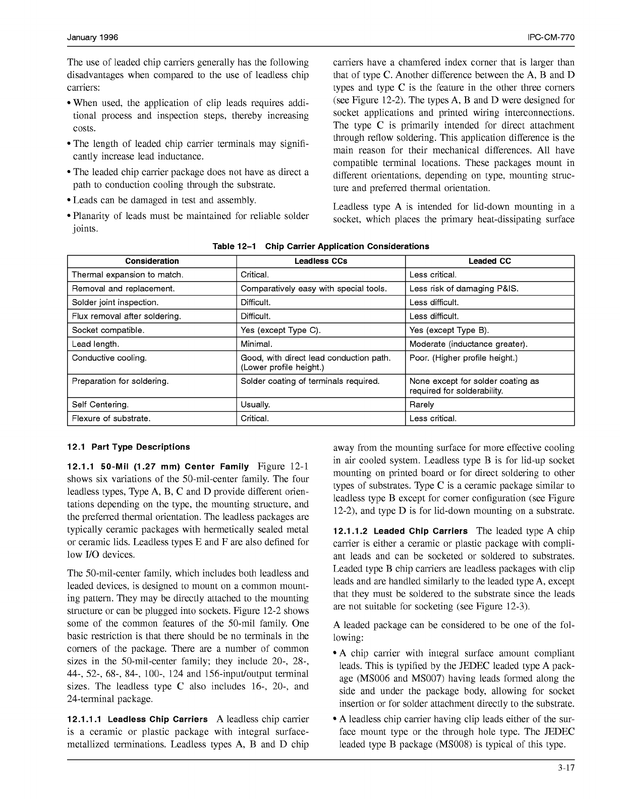
12.1.1 50-Mil (1.27 mm) Center Family
Figure 12-1
shows six variations of the 50-mil-center family. The four
leadless types, Type A,
B,
C and D provide different orien-
tations depending on the type, the mounting structure, and
the preferred thermal orientation. The leadless packages are
typically ceramic packages with hermetically sealed metal
or ceramic lids. Leadless types E and
F
are also defined for
low
I/O
devices.
The 50-mil-center family, which includes both leadless and
leaded devices, is designed to mount on a common mount-
ing pattern. They may be directly attached to the mounting
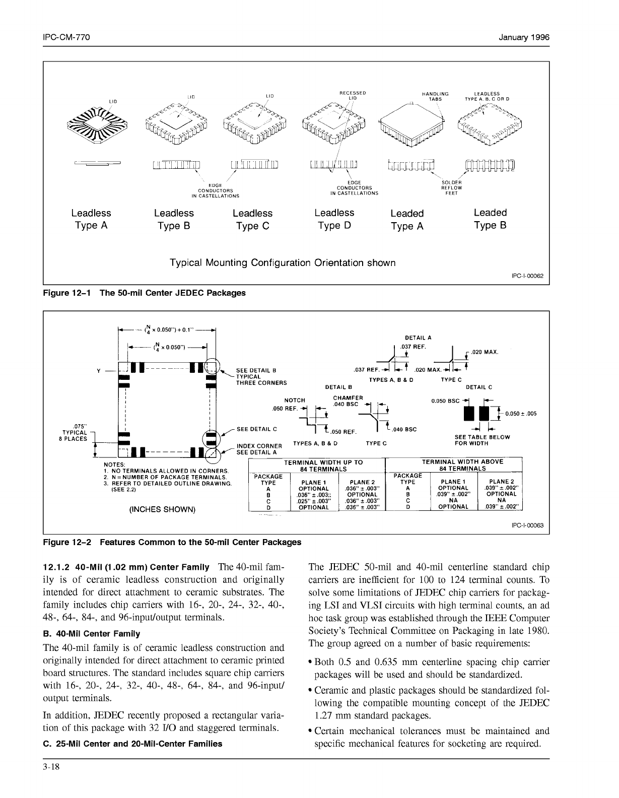
structure or can be plugged into sockets. Figure 12-2 shows
some of the common features of the 50-mil family. One
basic restriction is that there should be no terminals in the
comers of the package. There are a number of common
sizes in the 50-mil-center family; they include 20-, 28-,
44-, 52-, 68-, 84-,
loo-,
124 and 156-inpudoutput terminal
sizes. The leadless type C also includes 16-, 20-, and
24-terminal package.
12.1.1.1 Leadless Chip Carriers
A leadless chip carrier
is a ceramic or plastic package with integral surface-
metallized terminations. Leadless types A,
B
and D chip
away from the mounting surface for more effective cooling
in air cooled system. Leadless type
B
is for lid-up socket
mounting on printed board or for direct soldering to other
types of substrates. Type C is a ceramic package similar to
leadless type
B
except for comer configuration (see Figure
12-2), and type D is for lid-down mounting on a substrate.
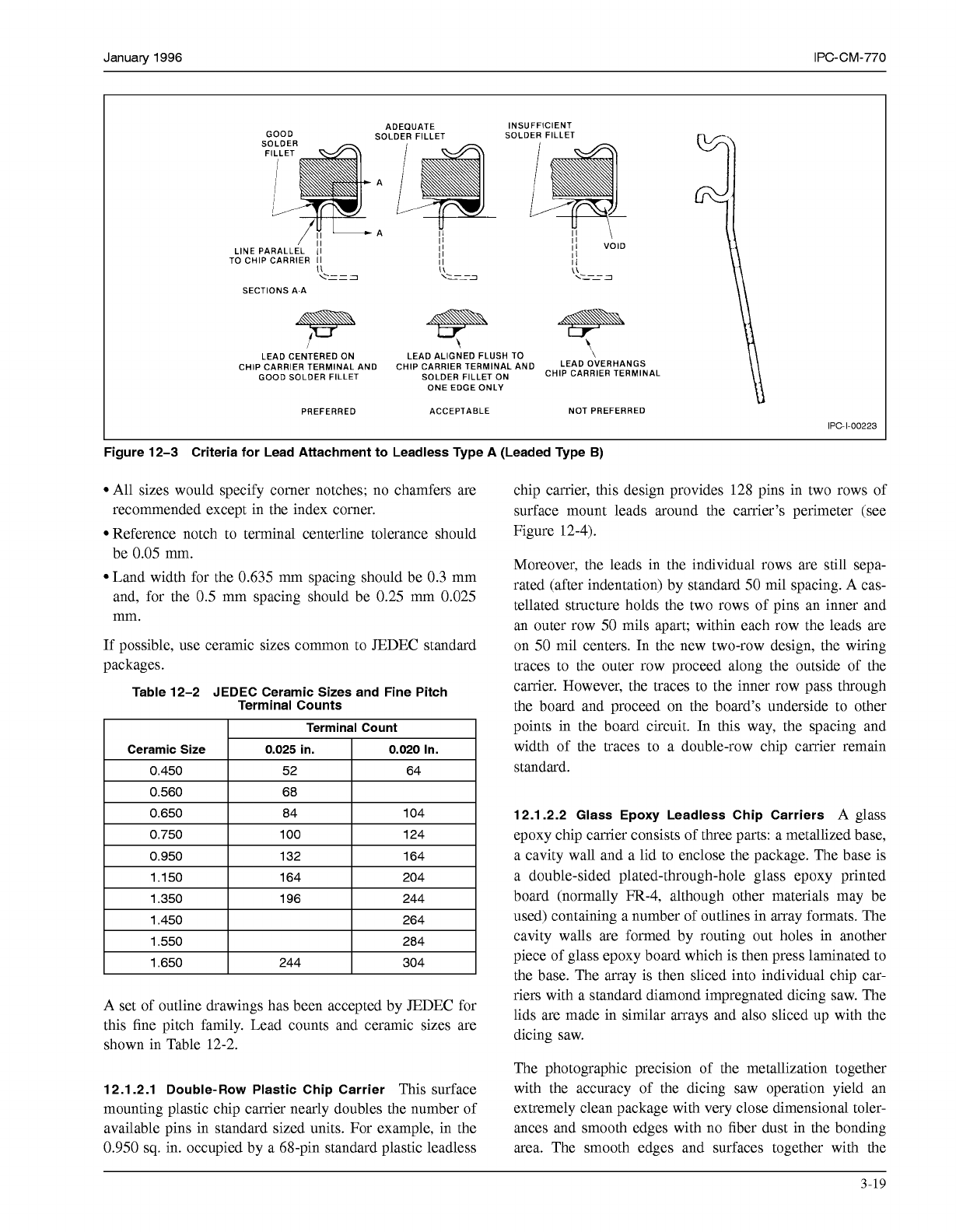
12.1.1.2 Leaded Chip Carriers
The leaded type A chip
carrier is either a ceramic or plastic package with compli-
ant leads and can be socketed or soldered to substrates.
Leaded type
B
chip carriers are leadless packages with clip
leads and are handled similarly to the leaded type A, except
that they must be soldered to the substrate since the leads
are not suitable for socketing (see Figure 12-3).
A leaded package can be considered to be one of the fol-
lowing:
A chip carrier with integral surface amount compliant
leads. This is typified by the JEDEC leaded type A pack-
age (MS006 and
MS007)
having leads formed along the
side and under the package body, allowing for socket
insertion or for solder attachment directly to the substrate.
A leadless chip carrier having clip leads either of the sur-
face mount type or the through hole type. The JEDEC
leaded type
B
package
(MS008)
is typical of this type.
3-17
COPYRIGHT Association Connecting Electronics Industries
Licensed by Information Handling Services
COPYRIGHT Association Connecting Electronics Industries
Licensed by Information Handling Services
IPC-CM-770
Januaty
1996
LIU
LID
RECESSED
HANDLING
LIU
TABS
TYPE A B.
C
OR
O
LEAOLESS
Leadless Leadless Leadless Leadless Leaded Leaded
Type
A
Type
B
Type
c
Type
D
Type
A
Type
B
Typical Mounting Configuration Orientation shown
IPC-I-O0062
Figure 12-1 The 50-mil Center JEDEC Packages
"
(y
x
0.050')
+
0.1"
DETAIL A
AT
REF.
JA
,020
MAX
SEE DETAIL B
.O37
REF.
4
b
,020
MAX.
4
m
THREE CORNERS
TYPICAL
TYPES A, B
&
D
TYPE
C
DETAIL B
DETAIL C
Ik,
NOTCH
CHAMFER
,050
REF.
yF+
TYPICAL
.075"
8
PLACES
J
SEE
c
llT.050
REF.
,040
ESC
AL
INDEX CORNER
TYPES
B
'
D
SEE TABLE BELOW
TYPE C
FOR
WIDTH
-7
I
-------
,I
J
SEE DETAIL A
NOTES:
PLANE
2
PLANE
1
TYPE
PLANE
2
PLANE
1
TYPE
3.
REFER TO DETAILED OUTLINE DRAWING.
PACKAGE
2.
N
=
NUMBER OF PACKAGE TERMINALS.
84 TERMINALS
1.
NO TERMINALS ALLOWED IN CORNERS.
TERMINAL WIDTH
UP
TO
TERMINAL WIDTH ABOVE
84 TERMINALS
PACKAGE
(SEE
2.2)
A
C
B
.039"?
,002"
OPTIONAL
OPTIONAL
,036"
f
,003;;
B
A
,036"
f
,003''
OPTIONAL
,039''
f.002"
OPTIONAL
D
NA
NA
.035"
,003"
OPTIONAL
D
C
,036'
?
.003"
,025"
f
.003"
OPTIONAL
,039'
?.002"
(INCHES SHOWN)
~~~ ~
IPC-I-O0063
Figure 12-2 Features Common to the 50-mil Center Packages
12.1.2 40-Mil (1 .O2 mm) Center Family
The 40-mil fam-
ily is of ceramic leadless construction and originally
intended for direct attachment to ceramic substrates. The
family includes chip carriers with 16-, 20-, 24-, 32-, 40-,
48-, 64-, 84-, and 96-inpudoutput terminals.
B.
40-Mil Center Family
The 40-mil family is of ceramic leadless construction and
originally intended for direct attachment to ceramic printed
board structures. The standard includes square chip carriers
with 16-, 20-, 24-, 32-, 40-, 48-, 64-, 84-, and 96-inpud
output terminals.
In addition, JEDEC recently proposed a rectangular varia-
tion of this package with 32
Il0
and staggered terminals.
C. 25-Mil Center and 20-Mil-Center Families
The JEDEC 50-mil and 40-mil centerline standard chip
carriers are inefficient for
100
to 124 terminal counts. To
solve some limitations of JEDEC chip carriers for packag-
ing LSI and VLSI circuits with high terminal counts, an ad
hoc task group was established through the IEEE Computer
Society's Technical Committee on Packaging in late 1980.
The group agreed on a number of basic requirements:
Both
0.5
and 0.635 mm centerline spacing chip carrier
packages will be used and should be standardized.
Ceramic and plastic packages should be standardized fol-
lowing the compatible mounting concept of the JEDEC
1.27 mm standard packages.
Certain mechanical tolerances must be maintained and
specific mechanical features for socketing are required.
3-18
COPYRIGHT Association Connecting Electronics Industries
Licensed by Information Handling Services
COPYRIGHT Association Connecting Electronics Industries
Licensed by Information Handling Services
January
1996
IPC-CM-770
GOOD
ADEQUATE
SOLDER FILLET
INSUFFICIENT
SOLDER FILLET
A
A
LINE PARALLEL
II
TO CHIP CARRIER
II
II
II
II
VOID
Il
Il
'"
-
-
".-
-
\"I
I'.-
-
\"
3
,"
3
SECTIONS A-A
LEAD CENTERED ON LEAD ALIGNED FLUSH TO
CHIP CARRIER TERMINAL AND CHIP CARRIER TERMINAL AND
LEAD
OVERHANGS
\
GOOD SOLDER FILLET
SOLDER
oN
CHIP CARRIER TERMINAL
ONE EDGE ONLY
PREFERRED ACCEPTABLE NOT PREFERRED
IPC-1-00223
Figure 12-3 Criteria for Lead Attachment to Leadless Type A (Leaded Type
B)
All sizes would specify comer notches; no chamfers are
recommended except in the index comer.
Reference notch to terminal centerline tolerance should
be
0.05
mm.
Land width for the 0.635 mm spacing should be 0.3 mm
and, for the
0.5
mm spacing should be 0.25 mm 0.025
mm.
If possible, use ceramic sizes common to JEDEC standard
packages.
Table 12-2 JEDEC Ceramic Sizes and Fine Pitch
Terminal Counts
A set of outline drawings has been accepted by JEDEC for
this fine pitch family. Lead counts and ceramic sizes are
shown in Table 12-2.
12.1.2.1 Double-Row Plastic Chip Carrier
This surface
mounting plastic chip carrier nearly doubles the number of
available pins in standard sized units. For example, in the
0.950
sq.
in. occupied by a 68-pin standard plastic leadless
chip carrier, this design provides 128 pins in two rows of
surface mount leads around the carrier's perimeter (see
Figure 12-4).
Moreover, the leads in the individual rows are still sepa-
rated (after indentation) by standard
50
mil spacing. A cas-
tellated structure holds the two rows of pins an inner and
an outer row
50
mils apart; within each row the leads are
on
50
mil centers. In the new two-row design, the wiring
traces to the outer row proceed along the outside of the
carrier. However, the traces to the inner row pass through
the board and proceed on the board's underside to other
points in the board circuit. In this way, the spacing and
width of the traces to a double-row chip carrier remain
standard.
12.1.2.2 Glass Epoxy Leadless Chip Carriers
A glass
epoxy chip carrier consists of three parts: a metallized base,
a cavity wall and a lid to enclose the package. The base is
a double-sided plated-through-hole glass epoxy printed
board (normally FR-4, although other materials may be
used) containing a number of outlines in array formats. The
cavity walls are formed by routing out holes in another
piece of glass epoxy board which is then press laminated to
the base. The array is then sliced into individual chip car-
riers with a standard diamond impregnated dicing saw. The
lids are made in similar arrays and also sliced up with the
dicing saw.
The photographic precision of the metallization together
with the accuracy of the dicing saw operation yield an
extremely clean package with very close dimensional toler-
ances and smooth edges with no fiber dust in the bonding
area. The smooth edges and surfaces together with the
3-19
COPYRIGHT Association Connecting Electronics Industries
Licensed by Information Handling Services
COPYRIGHT Association Connecting Electronics Industries
Licensed by Information Handling Services