IPC-CM-770D-1996 - 第56页
IPC-CM-770 Januaty 1996 close tolerances make these packages particularly adapt- able to automatic assembly, testing and handling equip- ment. The conductors consist of clad copper which is electro- plated with copper to…
January
1996
IPC-CM-770
GOOD
ADEQUATE
SOLDER FILLET
INSUFFICIENT
SOLDER FILLET
A
A
LINE PARALLEL
II
TO CHIP CARRIER
II
II
II
II
VOID
Il
Il
'"
-
-
".-
-
\"I
I'.-
-
\"
3
,"
3
SECTIONS A-A
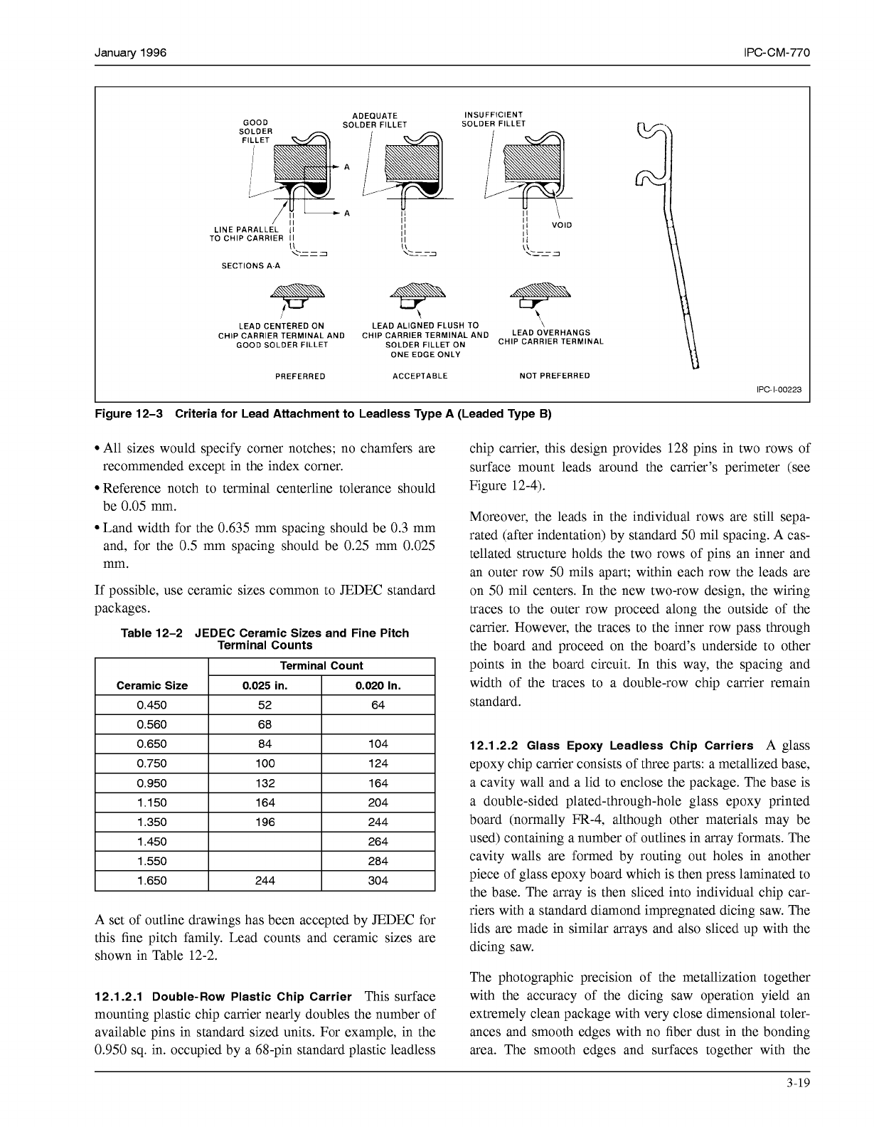
LEAD CENTERED ON LEAD ALIGNED FLUSH TO
CHIP CARRIER TERMINAL AND CHIP CARRIER TERMINAL AND
LEAD
OVERHANGS
\
GOOD SOLDER FILLET
SOLDER
oN
CHIP CARRIER TERMINAL
ONE EDGE ONLY
PREFERRED ACCEPTABLE NOT PREFERRED
IPC-1-00223
Figure 12-3 Criteria for Lead Attachment to Leadless Type A (Leaded Type
B)
All sizes would specify comer notches; no chamfers are
recommended except in the index comer.
Reference notch to terminal centerline tolerance should
be
0.05
mm.
Land width for the 0.635 mm spacing should be 0.3 mm
and, for the
0.5
mm spacing should be 0.25 mm 0.025
mm.
If possible, use ceramic sizes common to JEDEC standard
packages.
Table 12-2 JEDEC Ceramic Sizes and Fine Pitch
Terminal Counts
A set of outline drawings has been accepted by JEDEC for
this fine pitch family. Lead counts and ceramic sizes are
shown in Table 12-2.
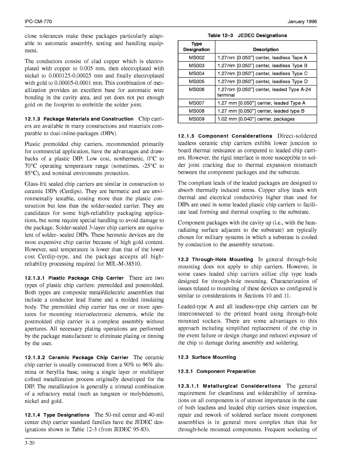
12.1.2.1 Double-Row Plastic Chip Carrier
This surface
mounting plastic chip carrier nearly doubles the number of
available pins in standard sized units. For example, in the
0.950
sq.
in. occupied by a 68-pin standard plastic leadless
chip carrier, this design provides 128 pins in two rows of
surface mount leads around the carrier's perimeter (see
Figure 12-4).
Moreover, the leads in the individual rows are still sepa-
rated (after indentation) by standard
50
mil spacing. A cas-
tellated structure holds the two rows of pins an inner and
an outer row
50
mils apart; within each row the leads are
on
50
mil centers. In the new two-row design, the wiring
traces to the outer row proceed along the outside of the
carrier. However, the traces to the inner row pass through
the board and proceed on the board's underside to other
points in the board circuit. In this way, the spacing and
width of the traces to a double-row chip carrier remain
standard.
12.1.2.2 Glass Epoxy Leadless Chip Carriers
A glass
epoxy chip carrier consists of three parts: a metallized base,
a cavity wall and a lid to enclose the package. The base is
a double-sided plated-through-hole glass epoxy printed
board (normally FR-4, although other materials may be
used) containing a number of outlines in array formats. The
cavity walls are formed by routing out holes in another
piece of glass epoxy board which is then press laminated to
the base. The array is then sliced into individual chip car-
riers with a standard diamond impregnated dicing saw. The
lids are made in similar arrays and also sliced up with the
dicing saw.
The photographic precision of the metallization together
with the accuracy of the dicing saw operation yield an
extremely clean package with very close dimensional toler-
ances and smooth edges with no fiber dust in the bonding
area. The smooth edges and surfaces together with the
3-19
COPYRIGHT Association Connecting Electronics Industries
Licensed by Information Handling Services
COPYRIGHT Association Connecting Electronics Industries
Licensed by Information Handling Services
IPC-CM-770 Januaty 1996
close tolerances make these packages particularly adapt-
able to automatic assembly, testing and handling equip-
ment.
The conductors consist of clad copper which is electro-
plated with copper to
0.005
mm, then electroplated with
nickel to 0.000125-0.00025 mm and finally electroplated
with gold to
0.00005-0.0001
mm. This combination of met-
allization provides an excellent base for automatic wire
bonding in the cavity area, and yet does not put enough
gold on the footprint to embrittle the solder joint.
12.1.3 Package Materials and Construction
Chip carri-
ers are available in many constructions and materials com-
parable to dual-inline-packages (DIPs).
Plastic premolded chip carriers, recommended primarily
for commercial application, have the advantages and draw-
backs of a plastic DIP: Low cost, nonhermetic, 0°C to
70°C operating temperature range (sometimes, -25°C to
85”C), and nominal environment protection.
Glass-frit sealed chip carriers are similar in construction to
ceramic DIPs (Cerdips). They are hermetic and are envi-
ronmentally testable, costing more than the plastic con-
struction but less than the solder-sealed carrier. They are
candidates for some high-reliability packaging applica-
tions, but some require special handling to avoid damage to
the package. Solder-sealed 3-layer chip carriers are equiva-
lent of solder- sealed DIPs. These hermetic devices are the
most expensive chip carrier because of high gold content.
However, seal temperature is lower than that of the lower
cost Cerdip-type, and the package accepts all high-
reliability processing required for MIL-M-385
10.
12.1.3.1 Plastic Package Chip Carrier
There are two
types of plastic chip carriers: premolded and postmolded.
Both types are composite metaUdielectric assemblies that
include a conductor lead frame and a molded insulating
body. The premolded chip carrier has one or more aper-
tures for mounting microelectronic elements, while the
postmolded chip carrier is a complete assembly without
apertures. All necessary plating operations are performed
by the package manufacturer to eliminate plating or tinning
by the user.
12.1.3.2 Ceramic Package Chip Carrier
The ceramic
chip carrier is usually constructed from a 90% to 96% alu-
mina or beryllia base, using a single layer or multilayer
cofired metallization process originally developed for the
DIP. The metallization is generally a trimetal combination
of a refractory metal (such as tungsten or molybdenum),
nickel and gold.
12.1.4 Type Designations
The 50-mil center and 40-mil
center chip carrier standard families have the JEDEC des-
ignations shown in Table 12-3 (from JEDEC 95-83).
Table 12-3 JEDEC Designations
Type
Designation Description
MS002
1.27mm [0.050”] center, leaded Type A-24 MS006
1.27mm [0.050”] center, leadless Type
D
MS005
1.27mm [0.050”] center, leadless Type C MS004
1.27mm [0.050”] center, leadless Type
B
MS003
1.27mm [0.050”] center, leadless Tape A
MS007 1.27 mm [0.050”] center, leaded Type A
MS008 1.27 mm [0.050”] center, leaded type
B
MS009 1 .O2 mm [0.040”] center, packages
terminal
12.1.5 Component Considerations
Direct-soldered
leadless ceramic chip carriers exhibit lower junction to
board thermal resistance as compared to leaded chip carri-
ers. However, the rigid interface is more susceptible to sol-
der joint cracking due to thermal expansion mismatch
between the component packages and the substrate.
The compliant leads of the leaded packages are designed to
absorb thermally induced stress. Copper alloy leads with
thermal and electrical conductivity higher than used for
DIPs are used in some leaded plastic chip carriers to facili-
tate lead forming and thermal coupling to the substrate.
Component packages with the cavity up (i.e., with the heat-
radiating surface adjacent to the substrate) are typically
chosen for military systems in which a substrate is cooled
by conduction to the assembly structure.
12.2 Through-Hole Mounting
In general through-hole
mounting does not apply to chip carriers. However, in
some cases leaded chip carriers utilize clip type leads
designed for through-hole mounting. Characterization of
issues related to mounting of these devices
so
configured is
similar to considerations in Sections
10
and
11.
Leaded-type A and all leadless-type chip carriers can be
interconnected to the printed board using through-hole
mounted sockets. There are some advantages to this
approach including simplified replacement of the chip in
the event failure or design change and reduced exposure of
the chip to damage during assembly and soldering.
12.3 Surface Mounting
12.3.1 Component Preparation
12.3.1.1 Metallurgical Considerations
The general
requirement for cleanliness and solderability of termina-
tions on all components is of utmost importance in the case
of both leadless and leaded chip carriers since inspection,
repair and rework of soldered surface mount component
assemblies is in general more complex than that for
through-hole mounted components. Frequent socketing of
3
-20
COPYRIGHT Association Connecting Electronics Industries
Licensed by Information Handling Services
COPYRIGHT Association Connecting Electronics Industries
Licensed by Information Handling Services
January
1996
IPC-CM-770
IPC-I-
Figure 12-4 Double
Row
Plastic Chip Carrier
ADEQUATE
GOOD SOLDER FILLET
A
LINE PARALLEL
Il
TO CHIP CARRIER
II
SOLDER FILLET
INSUFFICIENT
LEAD CENTERED ON
GOOD SOLDER FILLET
CHIP CARRIER TERMINAL AND CHIP CARRIER TERMINAL AND
LEAD
OVERHANGS
LEAD ALIGNED FLUSH
TO
\
SOLDER
oN
CHIP CARRIER TERMINAL
\\
ONE EDGE ONLY
PREFERRED ACCEPTABLE NOT PREFERRED
IPC-1-00223
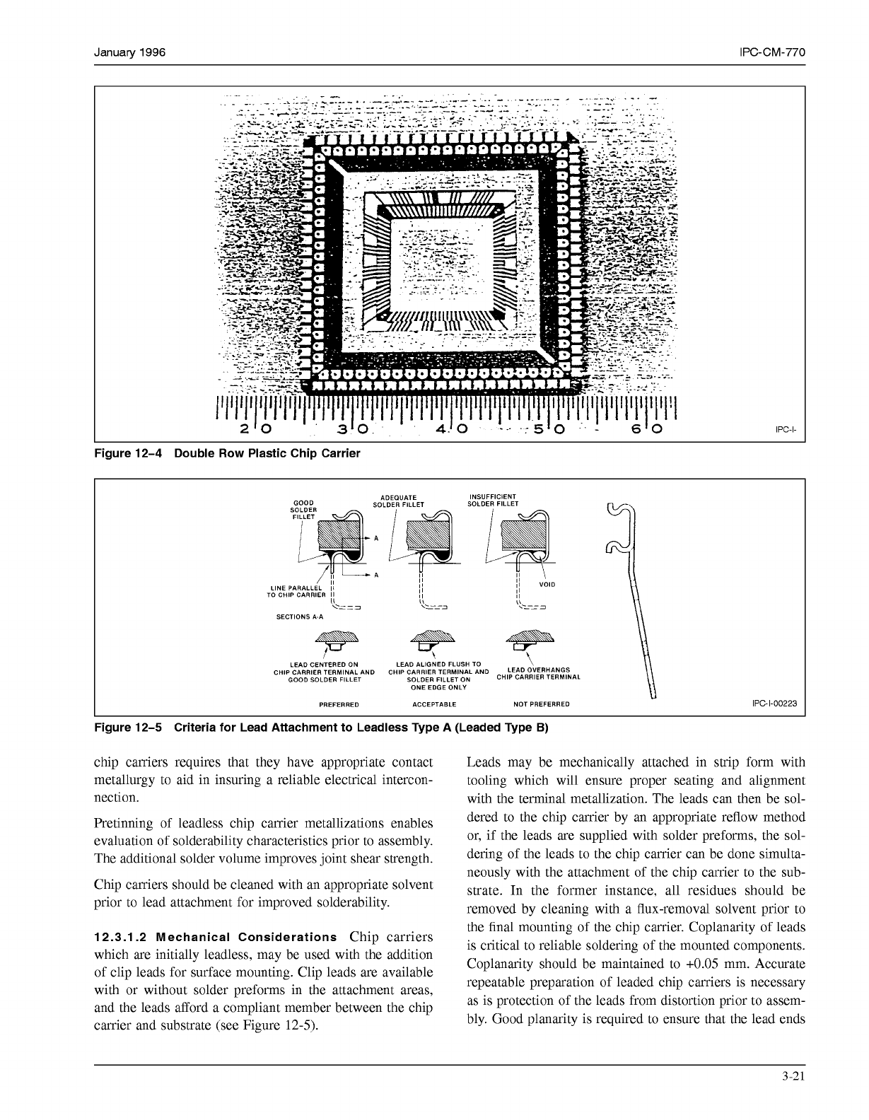
Figure 12-5 Criteria for Lead Attachment to Leadless Type A (Leaded Type
B)
chip carriers requires that they have appropriate contact
metallurgy to aid in insuring a reliable electrical intercon-
nection.
Pretinning of leadless chip carrier metallizations enables
evaluation of solderability characteristics prior to assembly.
The additional solder volume improves joint shear strength.
Chip carriers should be cleaned with an appropriate solvent
prior to lead attachment for improved solderability.
12.3.1.2 Mechanical Considerations
Chip carriers
which are initially leadless, may be used with the addition
of clip leads for surface mounting. Clip leads are available
with or without solder preforms in the attachment areas,
and the leads afford a compliant member between the chip
carrier and substrate (see Figure
12-5).
Leads may be mechanically attached in strip form with
tooling which will ensure proper seating and alignment
with the terminal metallization. The leads can then be sol-
dered to the chip carrier by an appropriate reflow method
or, if the leads are supplied with solder preforms, the sol-
dering of the leads to the chip carrier can be done simulta-
neously with the attachment of the chip carrier to the sub-
strate. In the former instance, all residues should be
removed by cleaning with a flux-removal solvent prior to
the final mounting of the chip carrier. Coplanarity of leads
is critical to reliable soldering of the mounted components.
Coplanarity should be maintained to
+0.05
mm. Accurate
repeatable preparation of leaded chip carriers is necessary
as is protection of the leads from distortion prior to assem-
bly. Good planarity is required to ensure that the lead ends
3-21
COPYRIGHT Association Connecting Electronics Industries
Licensed by Information Handling Services
COPYRIGHT Association Connecting Electronics Industries
Licensed by Information Handling Services