IPC-CM-770D-1996 - 第60页
IPC-CM-770 Januaty 1996 DIPS. This should extend the useful life of present day technology for some high lead count applications. soot- .OSO' SOLID CRlD I I l lo' 50 110 110 id0 II0 300 PACKAQE LEAD COUNT Ipc.I…
January
1996
IPC-CM-770
12.9 Cleaning
General techniques for cleaning applying
to all types of components are described in Section 28.
Because of generally smaller spacing between leads,
smaller clearances between substrate and the component
body, and large area beneath the devices, chip carriers
present a more difficult cleaning situation than through-
hole mounted devices. Clearance under the package should
be adequate to facilitate an effective cleaning operation.
Some surface mounting soldering processes result in
exposing the fluxes to high heat for longer and repeated
periods of time than experienced with through-hole compo-
nent soldering. This can lead to a more stable flux residue
making the cleaning more difficult. There is generally less
flux residue associated with chip carriers, but it is concen-
trated in smaller crevices under and between close spaced
devices.
Techniques using azeotropic solvents, aqueous cleaning
with detergents, as well as combinations of aqueous and
solvent cleaning process have been successfully applied.
12.10 Conformal Coating
General techniques for con-
formal coating for all types of assemblies are described in
Section 29.
13.0 AREA ARRAY COMPONENTS
The advent of very large scale integration (VLSI) and very
high speed integrated circuit (VHSIC) has brought a need
for very high pin count packages with lead symmetry and
methods to reliably assemble them onto circuit boards.
Grid arrays are pinned or leadless carriers with I/O contacts
that populate one surface of the package on a
0.100
inch
(eventually
0.050
inch) grid. The use of a solid grid neces-
sitates placing the die cavity on the side opposite the
Il0
contacts.
A
double or multiple concentric row grid permits
having die cavity and
Il0
contacts on the same side with
an optional heat sink on the opposite side.
13.1 Pin Grid Array Components
13.1.1 Port Types
The pin grid array package is the
package designed for high pin out ICs for through-hole
mounting because of its space efficiency and compatibility
with existing DIP facilities.
The main advantage of the pin-array is to avoid the
Il0
limitations of peripherally terminated packages such as
LCC at the same time providing terminal separations of
100-mil centerlines.
As
such it can be readily installed into
a conventional printed board and also wave soldered.
Offset disadvantages which have to be weighed:
Inspection of solder joints
Impedance limitations
Removal and replacement
A
typical pin grid array is a square, multilayer (usually
ceramic package having terminals on 2.54 x 2.54 mm cen-
ters. These packages are available in either cavity up or
cavity down versions.
A
cavity up configuration mounts the die opposite the pins,
thereby allowing a full grid of pins and the highest I/O
density.
A
cavity down configuration has the die on the same side
as the pins and is generally used with high power circuits
in air cooled applications to allow a heat sink opposite the
die. However, this version is not as space efficient.
Pin grid arrays have good electrical characteristics due to
the short signal paths from I/O pin to die. Pin grid arrays
overcome thermal expansion problems typically encoun-
tered at ceramic/printed board interfaces because the pins
are compliant. Conventional soldering techniques such as
wave soldering can attach these packages to printed boards.
The higher the I/O lead count becomes, the lower the per-
centage of the total package area any given-size die cavity
will occupy, e.g., the 96-lead, 40-mil center chip carrier is
over one-inch square.
For optimum packaging density, this percentage should be
as high as possible. Therefore, 0.635 and
0.5
mm chip car-
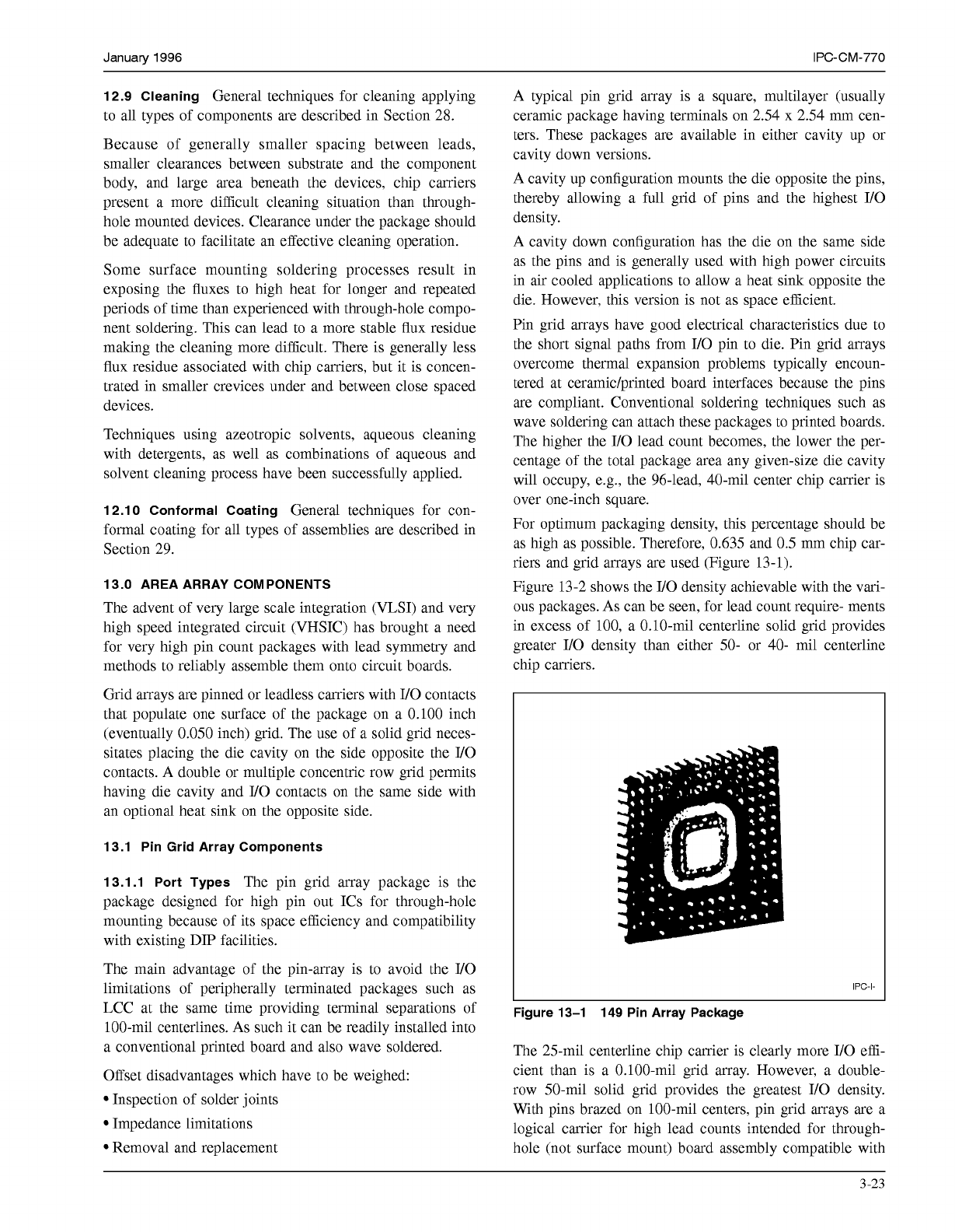
riers and grid arrays are used (Figure 13-1).
Figure 13-2 shows the
Il0
density achievable with the vari-
ous packages.
As
can be seen, for lead count require- ments
in excess of
100,
a 0.10-mil centerline solid grid provides
greater I/O density than either
50-
or 40- mil centerline
chip carriers.
IPC-I-
Figure 13-1 149 Pin Array Package
The 25-mil centerline chip carrier is clearly more I/O effi-
cient than is a 0.100-mil grid array. However, a double-
row 50-mil solid grid provides the greatest I/O density.
With pins brazed on 100-mil centers, pin grid arrays are a
logical carrier for high lead counts intended for through-
hole (not surface mount) board assembly compatible with
3-23
COPYRIGHT Association Connecting Electronics Industries
Licensed by Information Handling Services
COPYRIGHT Association Connecting Electronics Industries
Licensed by Information Handling Services
IPC-CM-770
Januaty
1996
DIPS. This should extend the useful life of present day
technology for some high lead count applications.
soot-
.OSO'
SOLID
CRlD
I
I
l
lo'
50
110
110
id0
II0
300
PACKAQE
LEAD
COUNT
Ipc.I.
L
Figure 13-2
110
Density Versus Lead Count (All
Dimensions in Inches)
13.1.2 Through-Hole Mounting
Through-hole mounting
is the dominant choice in pin grid array package applica-
tions.
Due to the high count of I/O pins the package can be
inserted in the present 100-mil grid through-hole process
and subjected to wave soldering.
Inspection of the solder connections under the package
body can be easily performed on the solder side of the
board and the device can be tested on existing "bed
of
nails" testers.
Inspecting the solder joints on the component side of the
board is extremely difficult without the aid of special tools
such as a fiber optic inspection system or a laser system
where joint temperature profile is indicative of the amount
of solder and integrity of the joint.
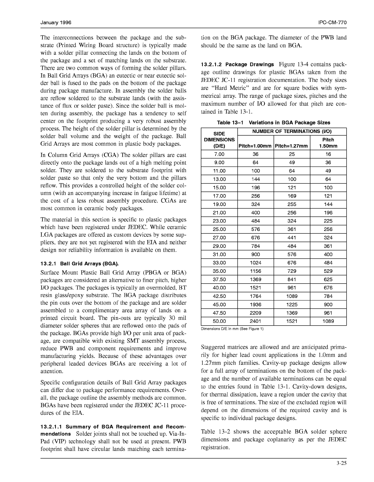
For this reason and because of the risks involved with
removal of these packages, sockets have been utilized (see
Figure
13-3).
Low profile grip sockets can also be used.
13.1.2.1 Component Preparation
Pin grid arrays con-
taining rigidized leads do not require lead forming prior to
assembly. They are through-hole mounted with straight
lead attach.
13.1.2.2 Land Patterns
When mounted directly to the
printed board, land patterns will be developed according to
the applicable class of the assembly. However, the lead
hole clearance should be
0.010-0.014
inch to allow for
placement variables and good capillary action of solder
flow.
Figure 13-3 Zero Insertion Force Socket
13.1.2.3 Lead Configuration After Assembly
Due to pin
density of pin grid array packages they can be mounted
with leads extending through the holes. Lead clinching is
not required.
13.1.3 Mixed Technology
The pin grid array being
through-hole mounted can be utilized along with other
through-hole components, DlPs, axial- leaded components,
etc. as part of a mixed assembly.
13.1.4 Manual Assembly
Manual assembly of the pin
grid array package to the printed board can be achieved by
using special tools designed for ease of alignment and
insertion. The operator can use a tweezer- type device to
place and hold a component, or a machine-positioned
vacuum pick-up under the operators control.
13.1.5 Automated Assembly
For high volume pin grid
array package assembly, high accuracy assembly robot
workcells represent a cost effective method of automating
semiautomatic and manual steps. The workcells can be
configured to perform a wide variety of insertion and
assembly tasks. Automated techniques for installing the
PGA to the board presently utilize robotic applications.
13.2 Surface Mount Area Arrays
This section provides
information on the design and assembly considerations for
the use of Surface Mount Grid Array packages. Generally,
they are known as Pad Grid Arrays or as Land Grid Arrays
(LGA). The terminations on the BGA packages are distrib-
uted over the bottom of the package and are solder
assembled to an area array of lands on a printed circuit
board. They are intended to provide high IO packaging of
integrated circuits in a small physical space with good reli-
ability, good assembly quality and low assembly cost.
Some have been registered under the JEDEC JC-11 proce-
dures of the EIA.
3
-24
COPYRIGHT Association Connecting Electronics Industries
Licensed by Information Handling Services
COPYRIGHT Association Connecting Electronics Industries
Licensed by Information Handling Services
January
1996
IPC-CM-770
The interconnections between the package and the sub-
strate (Printed Wiring Board structure) is typically made
with a solder pillar connecting the lands on the bottom of
the package and a set of matching lands on the substrate.
There are two common ways of forming the solder pillars.
In Ball Grid Arrays (BGA) an eutectic or near eutectic sol-
der ball is fused to the pads on the bottom of the package
during package manufacture. In assembly the solder balls
are reflow soldered to the substrate lands (with the assis-
tance of flux or solder paste). Since the solder ball is mol-
ten during assembly, the package has a tendency to self
center on the footprint producing a very robust assembly
process. The height of the solder pillar is determined by the
solder ball volume and the weight of the package. Ball
Grid Arrays are most common in plastic body packages.
In Column Grid Arrays (CGA) The solder pillars are cast
directly onto the package lands out of a high melting point
solder. They are soldered to the substrate footprint with
solder paste
so
that only the very bottom and the pillars
reflow. This provides a controlled height of the solder col-
umn (with an accompanying increase in fatigue lifetime) at
the cost of a less robust assembly procedure. CGAs are
most common in ceramic body packages.
The material in this section is specific to plastic packages
which have been registered under JEDEC. While ceramic
LGA packages are offered as custom devices by some sup-
pliers, they are not yet registered with the EIA and neither
design nor reliability information is available on them.
13.2.1 Ball Grid Arrays (BGA).
Surface Mount Plastic Ball Grid Array (PBGA or BGA)
packages are considered an alternative to finer pitch, higher
I/O packages. The packages is typically an overmolded, BT
resin glass/epoxy substrate. The BGA package distributes
the pin outs over the bottom of the package and are solder
assembled to a complimentary area array of lands on a
printed circuit board. The pin-outs are typically 30 mil
diameter solder spheres that are reflowed onto the pads of
the package. BGAs provide high I/O per unit area of pack-
age, are compatible with existing SMT assembly process,
reduce PWB and component requirements and improve
manufacturing yields. Because of these advantages over
peripheral leaded devices BGAs are receiving a lot of
attention.
Specific configuration details of Ball Grid Array packages
can differ due to package performance requirements. Over-
all, the package outline the assembly methods are common.
BGAs have been registered under the JEDEC JC-11 proce-
dures of the EIA.
13.2.1.1 Summary
of
BGA Requirement and Recom-
mendations
Solder joints shall not be touched up. Via-In-
Pad (VIP) technology shall not be used at present. PWB
footprint shall have circular lands matching each termina-
tion on the BGA package. The diameter of the PWB land
should be the same as the land on BGA.
13.2.1.2 Package Drawings
Figure 13-4 contains pack-
age outline drawings for plastic BGAs taken from the
JEDEC JC-11 registration documentation. The body sizes
are “Hard Metric” and are for square bodies with sym-
metrical array. The range of package sizes, pitches and the
maximum number of I/O allowed for that pitch are con-
tained in Table 13-1.
Table 13-1 Variations in BGA Package Sizes
Dimensions DIE in mm (See Figure
1)
Staggered matrices are allowed and are anticipated prima-
rily for higher lead count applications in the l.Omm and
1.27mm pitch families. Cavity-up package designs allow
for a full array of terminations on the bottom of the pack-
age and the number of available terminations can be equal
to the entries found in Table 13-1. Cavity-down designs,
for thermal dissipation, leave a region under the cavity that
is free of terminations. The size of the excluded region will
depend on the dimensions of the required cavity and is
specific to individual package designs.
Table 13-2 shows the acceptable BGA solder sphere
dimensions and package coplanarity as per the JEDEC
registration.
3-25
COPYRIGHT Association Connecting Electronics Industries
Licensed by Information Handling Services
COPYRIGHT Association Connecting Electronics Industries
Licensed by Information Handling Services