IPC-CM-770D-1996 - 第65页
January 1996 IPC-CM-770 Collector beam lead Base beam lead Emltter beam lead IPC-1-00349 Figure 14-3 Beam-lead Transistor Table 14-1 Various Chip Bonding Adhesive Types TY Pe Limitations Advantages Phenolics relatively h…
IPC-CM-770
Januaty
1996
i
*
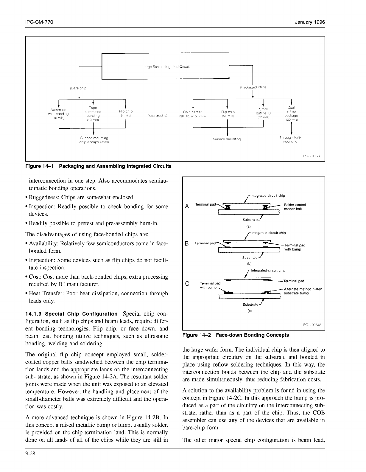
(Bare chlp)
b'acxnged
chIr:)
1
4
Autornatlc
wlre
bondlng
(10
111llb)
automated Fl~p
ch
p
D&
r
'
ne
bondlng
(10
r,'$
Chlp carrler
(4
TIIS)
FI
p
CIIP
Ilpan snacllg)
(20
40
or
50
1%)
(50
m
158
ouIlrie IC
(53
m
IS1
+
pat:
(100
r's!
chip encapsulatlon
Surface
mountlng
Surface mount
ng
Througi-
bole
mount
ng
IPC-1-00383
Figure 14-1 Packaging and Assembling Integrated Circuits
interconnection in one step. Also accommodates semiau-
tomatic bonding operations.
Ruggedness: Chips are somewhat enclosed.
Inspection: Readily possible to check bonding for some
devices.
Readily possible to pretest and pre-assembly bum-in.
The disadvantages of using face-bonded chips are:
Availability: Relatively few semiconductors come in face-
bonded form.
Inspection: Some devices such as flip chips do not facili-
tate inspection.
Cost: Cost more than back-bonded chips, extra processing
required by IC manufacturer.
Heat Transfer: Poor heat dissipation, connection through
leads only.
14.1.3 Special Chip Configuration
Special chip con-
figuration, such as flip chips and beam leads, require differ-
ent bonding technologies. Flip chip, or face down, and
beam lead bonding utilize techniques, such as ultrasonic
bonding, welding and soldering.
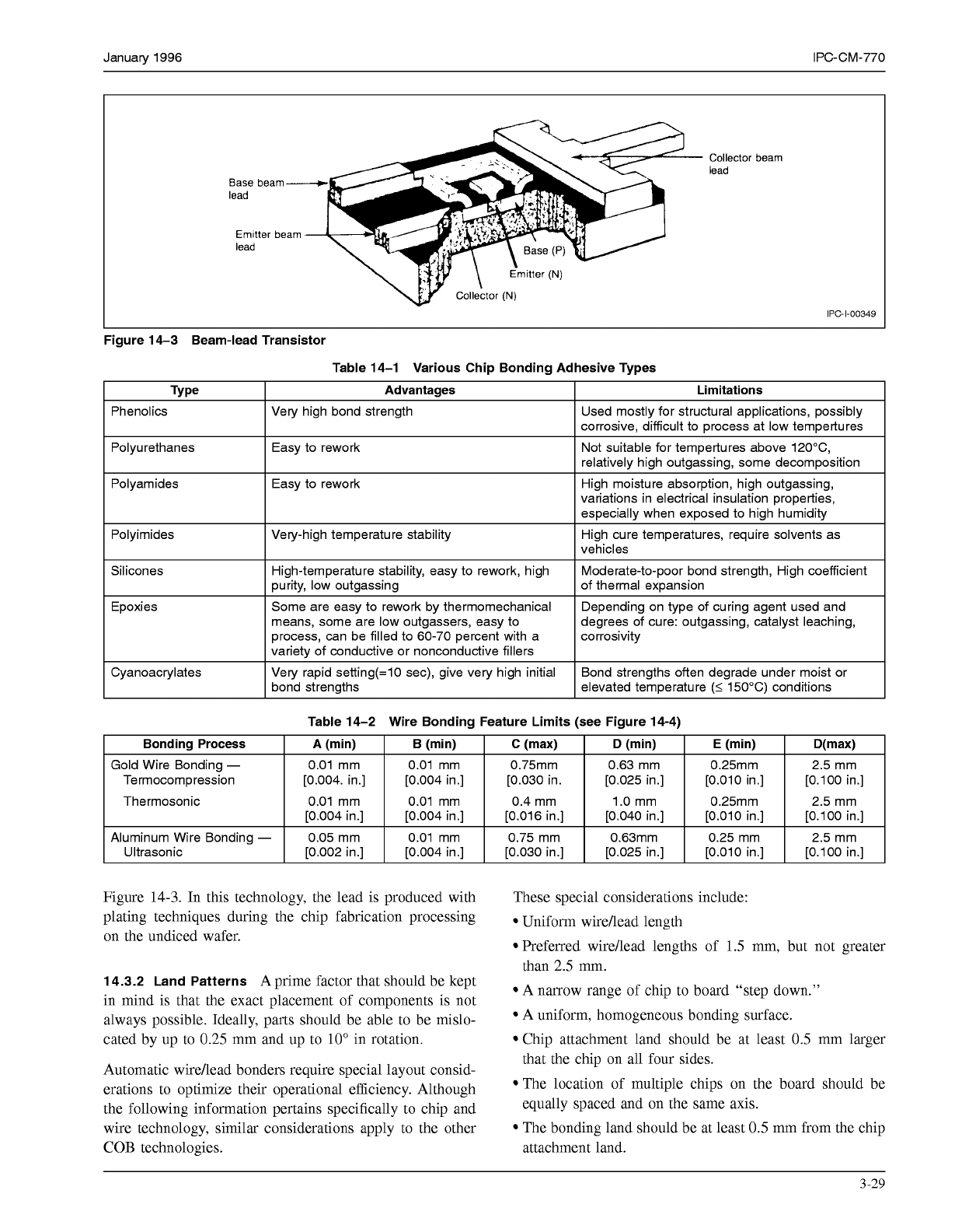
The original flip chip concept employed small, solder-
coated copper balls sandwiched between the chip termina-
tion lands and the appropriate lands on the interconnecting
sub- strate, as shown in Figure 14-2A. The resultant solder
joints were made when the unit was exposed to an elevated
temperature. However, the handling and placement of the
small-diameter balls was extremely difficult and the opera-
tion was costly.
A more advanced technique is shown in Figure 14-2B. In
this concept a raised metallic bump or lump, usually solder,
is provided on the chip termination land. This is normally
done on all lands of all of the chips while they are still in
Integrated-clrcult chlp
A
Termlnal pad
1
Solder coaled
I
v
copper ball
Substrate
(a)
r
Integrated-clrcult chlp
I
Substrate
(b)
lntegrated~clrcult chlp
r
a
c
Terminal pad
C-Termlnal pad
Alternate method plated
substrate bump
IPC-1-00348
gure 14-2 Face-down Bonding Concepts
the large wafer form. The individual chip is then aligned to
the appropriate circuitry on the substrate and bonded in
place using reflow soldering techniques. In this way, the
interconnection bonds between the chip and the substrate
are made simultaneously, thus reducing fabrication costs.
A solution to the availability problem is found in using the
concept in Figure 14-2C. In this approach the bump is pro-
duced as a part of the circuitry on the interconnecting sub-
strate, rather than as a part of the chip. Thus, the COB
assembler can use any of the devices that are available in
bare-chip form.
The other major special chip configuration is beam lead,
3-28
COPYRIGHT Association Connecting Electronics Industries
Licensed by Information Handling Services
COPYRIGHT Association Connecting Electronics Industries
Licensed by Information Handling Services
January 1996 IPC-CM-770
Collector beam
lead
Base beam
lead
Emltter beam
lead
IPC-1-00349
Figure 14-3 Beam-lead Transistor
Table 14-1 Various Chip Bonding Adhesive Types
TY Pe
Limitations
Advantages
Phenolics
relatively high outgassing, some decomposition
Not suitable for tempertures above 120"C, Easy to rework
Polyurethanes
corrosive, difficult to process at low tempertures
Used mostly for structural applications, possibly Very high bond strength
Polyamides
Easy to rework High moisture absorption, high outgassing,
variations in electrical insulation properties,
especially when exposed to high humidity
vehicles
Polyimides
of thermal expansion
purity, low outgassing
Moderate-to-poor bond strength, High coefficient High-temperature stability, easy to rework, high Silicones
High cure temperatures, require solvents as Very-high temperature stability
Epoxies
Some are easy to rework by thermomechanical Depending on type of curing agent used and
means, some are low outgassers, easy to degrees of cure: outgassing, catalyst leaching,
process, can be filled to 60-70 percent with a
variety of conductive or nonconductive fillers
corrosivity
bond strengths elevated temperature
(5
150°C) conditions
Cyanoacrylates
Bond strengths often degrade under moist or Very rapid setting(=lO sec), give very high initial
Table 14-2 Wire Bonding Feature Limits (see Figure 14-4)
Bonding Process
B (min) A (min)
Gold Wire Bonding
-
Termocompression
Thermosonic
0.01 mm
[0.004
in.]
[0.004
in.]
0.01 mm 0.01 mm
[0.004
in.]
[0.004.
in.]
0.01 mm
Aluminum Wire Bonding
-
0.01 mm
Ultrasonic
I
10.004
in.]
Figure
14-3.
In this technology, the lead is produced with
plating techniques during the chip fabrication processing
on the undiced wafer.
14.3.2 Land Patterns
A prime factor that should be kept
in mind is that the exact placement of components is not
always possible. Ideally, parts should be able to be mislo-
cated by up to
0.25
mm and up to
10"
in rotation.
Automatic wire/lead bonders require special layout consid-
erations to optimize their operational efficiency. Although
the following information pertains specifically to chip and
wire technology, similar considerations apply to the other
COB technologies.
C
(max)
I
D (min)
E
(min)
0.75mm 0.63 mm
[0.030 in. [0.025 in.]
0.4
mm 1
.O
mm
0.75 mm 0.63mm
0.25mm
[0.010 in.]
0.25mm
[0.010 in.]
0.25 mm
[0.010 in.]
D(max)
2.5 mm
[0.100 in.]
2.5 mm
[0.100 in.]
2.5 mm
[0.100 in.]
These special considerations include:
Uniform wireAead length
Preferred wire/lead lengths of
1.5
mm, but not greater
than
2.5
mm.
A narrow range of chip to board "step down."
A uniform, homogeneous bonding surface.
Chip attachment land should be at least
0.5
mm larger
that the chip on all four sides.
The location of multiple chips on the board should be
equally spaced and on the same axis.
The bonding land should be at least
0.5
mm from the chip
attachment land.
3-29
COPYRIGHT Association Connecting Electronics Industries
Licensed by Information Handling Services
COPYRIGHT Association Connecting Electronics Industries
Licensed by Information Handling Services
IPC-CM-770
Januaty
1996
The width of wireAead bonding land should be at least
0.25 mm by 0.75 mm.
Spacing between adjacent wireAeads should be 0.25 mm
minimum.
The tip of the bonding wireAead should have a square
configuration.
The soldermask opening should be at least 1.25 mm from
the edge of the bonding land.
Thermocompression ball bonding requires relatively-large
bond- ing lands and wire bonding clear- ances for high-
yieldhigh-rate production. Figure
14-4
shows the recom-
mended layout features and limits for the determination of
COB land patterns.
14.3.3 LeadlLand Configuration After Assembly
The
three basic chip attachment and termination techniques are
wire bonding (chip-and-wire), tape automated bonding
(TAB), and controlled collapse (Flip Chip) bonding.
14.4 Mixed Technology
The use of unpackaged semi-
conductor components is feasible in mixed assembly
technology.
L
\
Subslrale
Conduclor
t
IPC-I-
Figure 14-4 Wire Bonding Layout Features (see Table
14-2)
14.5 Manual Assembly
Manual techniques are usually
used for assembling special parts that may have one or two
type parts on a particular assembly. This relates to trans-
formers, relays, crystals, etc. When handling semiconduc-
tor device components, manual placement techniques usu-
ally require the addition of magnification. The small size
and fragility of bare chips used in COB technology makes
manual assembly somewhat difficult and in some types of
COB, such as TAB, impossible. The manual wire/lead
bonding operator can often inspect and compensate for
deficiencies in board layout and/or bonding surfaces, while
automatic machines require conservative design features
and uniformity of bonding surfaces. However, machine
assembly is most desirable, in order to obtain the high vol-
ume benefits of COB technology.
14.6 Automated Assembly
The chip-on-board assembly
industry has now begun to closely follow similar manufac-
turing methods and procedures of those already well estab-
lished in the semiconductor and printed circuit industries.
Various unique approaches have been taken to solve COB
manufacturing problems with cost-effective solutions for
the particular applications involved.
Automated techniques are usually not employed for mount-
ing special components, unless a large variety of the com-
ponents constitute an entire assembly. This might espe-
cially be true for chip on board technology, where many
chips might be mounted on a single interconnecting
substrate.
Special requirements for wire bonding and automated
assembly for chip on board are defined in Section 23.
14.7 Handling and Storage
The handling and storage of
unpackaged semiconductor components should be in accor-
dance with the guidelines of Section 26.
14.8 Soldering
Most COB technologies do not involve
the use of solder, with the exception of flip-chip. Flip chips
are soldered by means of reflow soldering techniques simi-
lar to that used for other packaged devices such as leaded
or leadless chip carriers.
When metal sealing lids are used as a chip protection
method, soldering is generally used to attach the lid to the
board. The use of preforms is often the most convenient
method for applying the solder. The heat required to reflow
the solder can be applied using one of the soldering pro-
cesses that is associated with conventional surface mount-
ing technology.
General soldering guidelines are discussed in Section 27.
14.9 Cleaning
Cleaning requirements associated with
soldered through-the-board and surface mounted assem-
blies, in most cases, do not apply to COB technology.
However, very stringent cleanliness requirements are
needed for the boards to be used for COB. Also, strict
cleanliness standards should be maintained in the assembly
3-30
COPYRIGHT Association Connecting Electronics Industries
Licensed by Information Handling Services
COPYRIGHT Association Connecting Electronics Industries
Licensed by Information Handling Services