IPC-CM-770D-1996 - 第67页
January 1996 IPC-CM-770 environment, since bare chips are being handled. General cleaning guidelines are discussed in Section 28. Attention should be placed on component and solvent compatibility. 14.1 O Coatings General…
IPC-CM-770
Januaty
1996
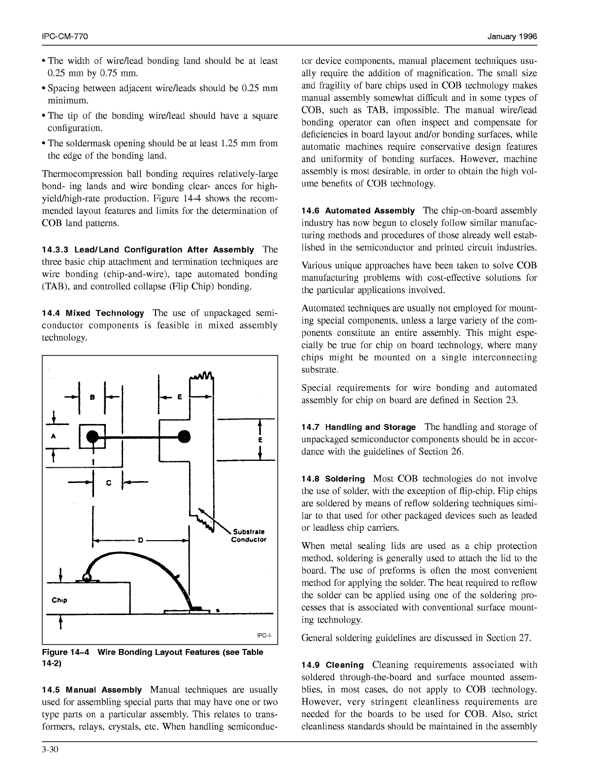
The width of wireAead bonding land should be at least
0.25 mm by 0.75 mm.
Spacing between adjacent wireAeads should be 0.25 mm
minimum.
The tip of the bonding wireAead should have a square
configuration.
The soldermask opening should be at least 1.25 mm from
the edge of the bonding land.
Thermocompression ball bonding requires relatively-large
bond- ing lands and wire bonding clear- ances for high-
yieldhigh-rate production. Figure
14-4
shows the recom-
mended layout features and limits for the determination of
COB land patterns.
14.3.3 LeadlLand Configuration After Assembly
The
three basic chip attachment and termination techniques are
wire bonding (chip-and-wire), tape automated bonding
(TAB), and controlled collapse (Flip Chip) bonding.
14.4 Mixed Technology
The use of unpackaged semi-
conductor components is feasible in mixed assembly
technology.
L
\
Subslrale
Conduclor
t
IPC-I-
Figure 14-4 Wire Bonding Layout Features (see Table
14-2)
14.5 Manual Assembly
Manual techniques are usually
used for assembling special parts that may have one or two
type parts on a particular assembly. This relates to trans-
formers, relays, crystals, etc. When handling semiconduc-
tor device components, manual placement techniques usu-
ally require the addition of magnification. The small size
and fragility of bare chips used in COB technology makes
manual assembly somewhat difficult and in some types of
COB, such as TAB, impossible. The manual wire/lead
bonding operator can often inspect and compensate for
deficiencies in board layout and/or bonding surfaces, while
automatic machines require conservative design features
and uniformity of bonding surfaces. However, machine
assembly is most desirable, in order to obtain the high vol-
ume benefits of COB technology.
14.6 Automated Assembly
The chip-on-board assembly
industry has now begun to closely follow similar manufac-
turing methods and procedures of those already well estab-
lished in the semiconductor and printed circuit industries.
Various unique approaches have been taken to solve COB
manufacturing problems with cost-effective solutions for
the particular applications involved.
Automated techniques are usually not employed for mount-
ing special components, unless a large variety of the com-
ponents constitute an entire assembly. This might espe-
cially be true for chip on board technology, where many
chips might be mounted on a single interconnecting
substrate.
Special requirements for wire bonding and automated
assembly for chip on board are defined in Section 23.
14.7 Handling and Storage
The handling and storage of
unpackaged semiconductor components should be in accor-
dance with the guidelines of Section 26.
14.8 Soldering
Most COB technologies do not involve
the use of solder, with the exception of flip-chip. Flip chips
are soldered by means of reflow soldering techniques simi-
lar to that used for other packaged devices such as leaded
or leadless chip carriers.
When metal sealing lids are used as a chip protection
method, soldering is generally used to attach the lid to the
board. The use of preforms is often the most convenient
method for applying the solder. The heat required to reflow
the solder can be applied using one of the soldering pro-
cesses that is associated with conventional surface mount-
ing technology.
General soldering guidelines are discussed in Section 27.
14.9 Cleaning
Cleaning requirements associated with
soldered through-the-board and surface mounted assem-
blies, in most cases, do not apply to COB technology.
However, very stringent cleanliness requirements are
needed for the boards to be used for COB. Also, strict
cleanliness standards should be maintained in the assembly
3-30
COPYRIGHT Association Connecting Electronics Industries
Licensed by Information Handling Services
COPYRIGHT Association Connecting Electronics Industries
Licensed by Information Handling Services
January
1996
IPC-CM-770
environment, since bare chips are being handled. General
cleaning guidelines are discussed in Section 28. Attention
should be placed on component and solvent compatibility.
14.1
O
Coatings
General conformal coating characteris-
tics applying to all types of components and assemblies are
described in Section 29.
Coatings are used in COB technology to protect the bonded
chips on the board from handling damage as well as for
environmental protection. Typical coatings used for this
purpose are room- temperature vulcanizing @TV) disper-
sion coatings, silicon dielectric gel, and epoxy type coat-
ings, applied locally at the bonded chip site, as opposed to
entire board coating.
14.10.1
RTV
Dispersion Coating
Typical RTV disper-
sion coatings are one-component, room-temperature vulca-
nizing (RTV) silicone-rubber coatings that are supplied as
a xylene dispersion.
(No
mixing is required.) The curing
process used a crosslinking mechanism that generates
methanol during cure. Once applied and exposed, the mate-
rial vulcanizes by reaction with moisture from the air to
form a soft, resilient elastomeric coating that will withstand
long term exposure to temperature as high as 250°C
(482°F).
14.10.2 Silicone Dielectric Gel
Special controlled tech-
nology can yield a silicone gel that affords the nonflowable
permanence of a solid, but also gives the freedom from
large mechanical and thermal stresses of a fluid. Chemi-
cally, a typical silicone gel is very similar to silicone flu-
ids, but with just enough crosslinking to prevent separation
of the individual polymer chains and give nonflow thermal-
set properties. The fully-cured dielectric gel is a soft, jelly-
like material that exhibits tenacious pressure-sensitive
adhesion to virtually any substrate.
14.10.3 Epoxy Coatings
Epoxy coatings are also avail-
able for COB self-crowning or “glob-top’’ applications.
Typical materials are two-component, liquid epoxy/
anhydride systems that have been formulated for their
superior thermal shock performance, substrate adhesion,
moisture resistance, and glass-transition temperatures in the
range of from
165”
to 180°C.
3-3
1
COPYRIGHT Association Connecting Electronics Industries
Licensed by Information Handling Services
COPYRIGHT Association Connecting Electronics Industries
Licensed by Information Handling Services
IPC-CM-770
Januaty
1996
3-32
COPYRIGHT Association Connecting Electronics Industries
Licensed by Information Handling Services
COPYRIGHT Association Connecting Electronics Industries
Licensed by Information Handling Services