IPC-CM-770D-1996 - 第81页
January 1996 IPC-CM-770 the inside. A post assembly terminal review should high- light lead length conformance and separation of lead ends from other leads or surface conductors. 16.2.2.1 Polarization The device and sock…
IPC-CM-770
Januaty
1996
.a35
Section
fhru
Contact
Cuvitv
IPC-I-
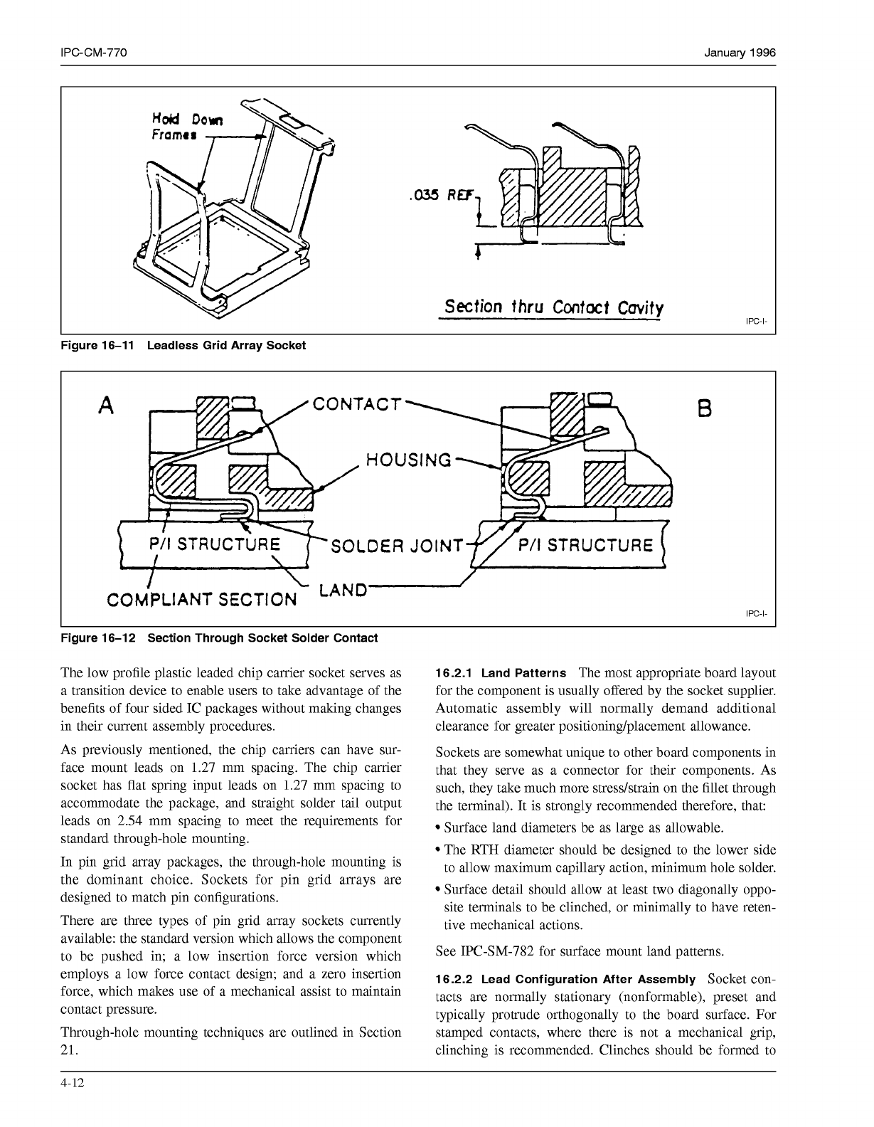
Figure 16-11 Leadless Grid Array Socket
A
r
'ACT-
HOUS
PA
STRUCTURE
?SOLDER
J
\
ING
OIN
T
P/I
STRUCTURE
COMPLIANT SECTION
L
LAND
B
IPC-I-
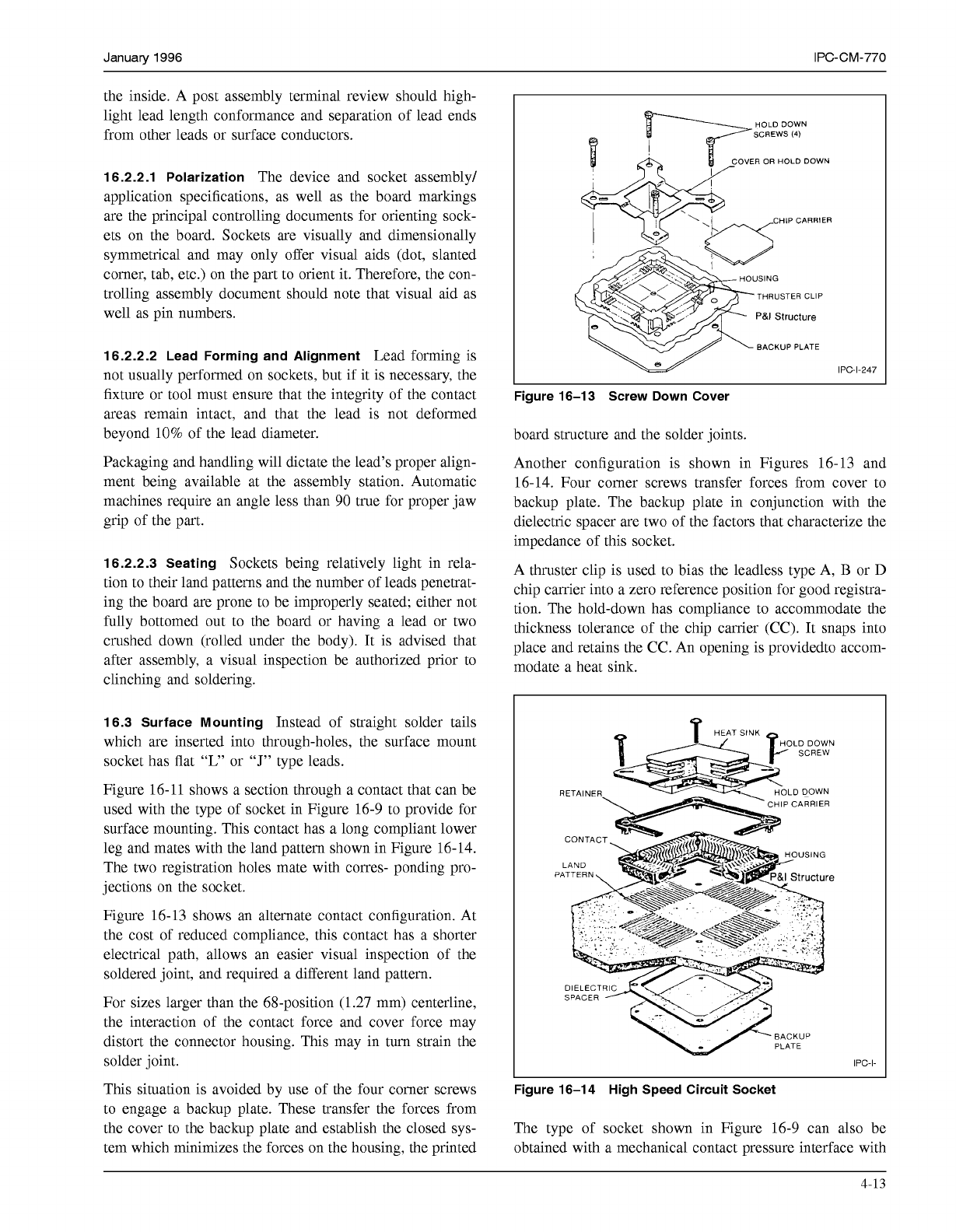
Figure 16-1 2 Section Through Socket Solder Contact
The low profile plastic leaded chip carrier socket serves as
a transition device to enable users to take advantage of the
benefits of four sided IC packages without making changes
in their current assembly procedures.
As previously mentioned, the chip carriers can have sur-
face mount leads on 1.27 mm spacing. The chip carrier
socket has flat spring input leads on 1.27 mm spacing to
accommodate the package, and straight solder tail output
leads on 2.54 mm spacing to meet the requirements for
standard through-hole mounting.
In pin grid array packages, the through-hole mounting is
the dominant choice. Sockets for pin grid arrays are
designed to match pin configurations.
There are three types of pin grid array sockets currently
available: the standard version which allows the component
to be pushed in; a low insertion force version which
employs a low force contact design; and a zero insertion
force, which makes use of a mechanical assist to maintain
contact pressure.
Through-hole mounting techniques are outlined in Section
21.
16.2.1 Land Patterns
The most appropriate board layout
for the component is usually offered by the socket supplier.
Automatic assembly will normally demand additional
clearance for greater positioning/placement allowance.
Sockets are somewhat unique to other board components in
that they serve as a connector for their components. As
such, they take much more stresdstrain on the fillet through
the terminal). It is strongly recommended therefore, that:
Surface land diameters be as large as allowable.
The RTH diameter should be designed to the lower side
to allow maximum capillary action, minimum hole solder.
Surface detail should allow at least two diagonally oppo-
site terminals to be clinched, or minimally to have reten-
tive mechanical actions.
See IPC-SM-782 for surface mount land patterns.
16.2.2 Lead Configuration After Assembly
Socket con-
tacts are normally stationary (nonformable), preset and
typically protrude orthogonally to the board surface. For
stamped contacts, where there is not a mechanical grip,
clinching is recommended. Clinches should be formed to
4-12
COPYRIGHT Association Connecting Electronics Industries
Licensed by Information Handling Services
COPYRIGHT Association Connecting Electronics Industries
Licensed by Information Handling Services
January
1996
IPC-CM-770
the inside. A post assembly terminal review should high-
light lead length conformance and separation of lead ends
from other leads or surface conductors.
16.2.2.1 Polarization
The device and socket assembly/
application specifications, as well as the board markings
are the principal controlling documents for orienting sock-
ets on the board. Sockets are visually and dimensionally
symmetrical and may only offer visual aids (dot, slanted
comer, tab, etc.) on the part to orient it. Therefore, the con-
trolling assembly document should note that visual aid as
well as pin numbers.
16.2.2.2 Lead Forming and Alignment
Lead forming is
not usually performed on sockets, but if it is necessary, the
fixture or tool must ensure that the integrity of the contact
areas remain intact, and that the lead is not deformed
beyond
10%
of the lead diameter.
Packaging and handling will dictate the lead’s proper align-
ment being available at the assembly station. Automatic
machines require an angle less than 90 true for proper jaw
grip of the part.
16.2.2.3 Seating
Sockets being relatively light in rela-
tion to their land patterns and the number of leads penetrat-
ing the board are prone to be improperly seated; either not
fully bottomed out to the board or having a lead or two
crushed down (rolled under the body). It is advised that
after assembly, a visual inspection be authorized prior to
clinching and soldering.
16.3 Surface Mounting
Instead of straight solder tails
which are inserted into through-holes, the surface mount
socket has flat
“L”
or
“J”
type leads.
Figure 16-11 shows a section through a contact that can be
used with the type of socket in Figure 16-9 to provide for
surface mounting. This contact has a long compliant lower
leg and mates with the land pattern shown in Figure 16-14.
The two registration holes mate with corres- ponding pro-
jections on the socket.
Figure 16-13 shows an alternate contact configuration. At
the cost of reduced compliance, this contact has a shorter
electrical path, allows an easier visual inspection of the
soldered joint, and required a different land pattern.
For sizes larger than the 68-position
(1.27
mm) centerline,
the interaction of the contact force and cover force may
distort the connector housing. This may in turn strain the
solder joint.
This situation is avoided by use of the four comer screws
to engage a backup plate. These transfer the forces from
the cover to the backup plate and establish the closed sys-
tem which minimizes the forces on the housing, the printed
HOLD
DOWN
SCREWS
(4)
COVER
OR
HOLD
DOWN
CHIP CARRIER
THRUSTER CLIP
BACKUP PLATE
IPC-I
-247
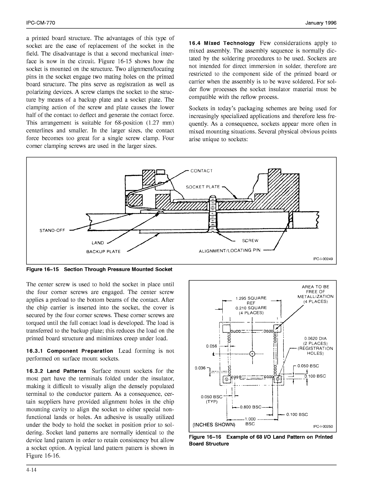
Figure 16-13 Screw Down Cover
board structure and the solder joints.
Another configuration is shown in Figures 16-13 and
16-14. Four comer screws transfer forces from cover to
backup plate. The backup plate in conjunction with the
dielectric spacer are two of the factors that characterize the
impedance of this socket.
A thruster clip is used to bias the leadless type A,
B
or
D
chip carrier into a zero reference position for good registra-
tion. The hold-down has compliance to accommodate the
thickness tolerance of the chip carrier
(CC).
It snaps into
place and retains the
CC.
An opening is providedto accom-
modate a heat sink.
IPC-I-
Figure 16-14 High Speed Circuit Socket
The type of socket shown in Figure 16-9 can also be
obtained with a mechanical contact pressure interface with
4-13
COPYRIGHT Association Connecting Electronics Industries
Licensed by Information Handling Services
COPYRIGHT Association Connecting Electronics Industries
Licensed by Information Handling Services
IPC-CM-770
Januaty
1996
a printed board structure. The advantages of this type of
socket are the ease of replacement of the socket in the
16.4 Mixed Technology
Few considerations apply to
field. The disadvantage is that a second mechanical inter-
mixed assembly. The assembly sequence is normally dic-
face is now in the circuit. Figure 16-15 shows how the
tated by the soldering procedures to be used. Sockets are
socket is mounted on the structure. Two alignmendlocating
not intended for direct immersion in solder, therefore are
pins in the socket engage two mating holes on the printed
restricted to the component side of the printed board or
board
The
pins
Serve
as
registration
as
well
as
carrier when the assembly is to be wave soldered. For sol-
devices.
A
Screw clamps
the
socket
to
the
strut-
der flow processes the socket insulator material must be
ture by means of a backup plate and a socket plate. The
with
the
reflow
process.
clamping action of the Screw and Plate causes the lower Sockets in today's packaging schemes are being used for
half of the Contact to deflect and generate the Contact force. increasingly specialized applications and therefore less fre-
This arrangement is suitable for 68-Position
(1.27
mm> quently. As a consequence, sockets appear more often in
centerlines and smaller. In the larger sizes, the contact mixed mounting situations. Several physical obvious points
force becomes too great for a single screw clamp. Four arise unique to sockets:
comer clamping screws are used in the larger sizes.
STAND-OFF
SOCKET PLATE
BACKUP PLATE ALIGNMENT/LOCATING PIN
IPC-I
-00249
Figure 16-15 Section Through Pressure Mounted Socket
The center screw is used to hold the socket in place until
the four comer screws are engaged. The center screw
applies a preload to the bottom beams of the contact. After
the chip carrier is inserted into the socket, the cover is
secured by the four comer screws. These comer screws are
torqued until the full contact load is developed. The load is
transferred to the backup plate; this reduces the load on the
printed board structure and minimizes creep under load.
16.3.1 Component Preparation
Lead forming is not
performed on surface mount sockets.
16.3.2 Land Patterns
Surface mount sockets for the
most part have the terminals folded under the insulator,
making it difficult to visually align the densely populated
terminal to the conductor pattern. As a consequence, cer-
tain suppliers have provided alignment holes in the chip
mounting cavity to align the socket to either special non-
functional lands or holes. An adhesive is usually utilized
under the body to hold the socket in position prior to sol-
dering. Socket land patterns are normally identical to the
device land pattern in order to retain consistency but allow
a socket option. A typical land pattern pattern is shown in
Figure 16- 16.
AREA TO BE
FREE OF
1
295 SQUARE
O
210
SQUARE
(4
PLACES)
METALLIZATION
REF
1
,(4
PLACES)
!Ll.OOO
---
(INCHES
SHOWN)
Esc IPC-I-O0250
Figure 16-16 Example
of
68
110
Land Pattern on Printed
Board Structure
4-14
COPYRIGHT Association Connecting Electronics Industries
Licensed by Information Handling Services
COPYRIGHT Association Connecting Electronics Industries
Licensed by Information Handling Services