IPC-CM-770D-1996 - 第83页
January 1996 IPC-CM-770 A. Heights Although low profile sockets are available, sockets (with their device) present a higher assembly pro- file. Wave solder holding plates are one point affected. B. Automatic Assembly As …
IPC-CM-770
Januaty
1996
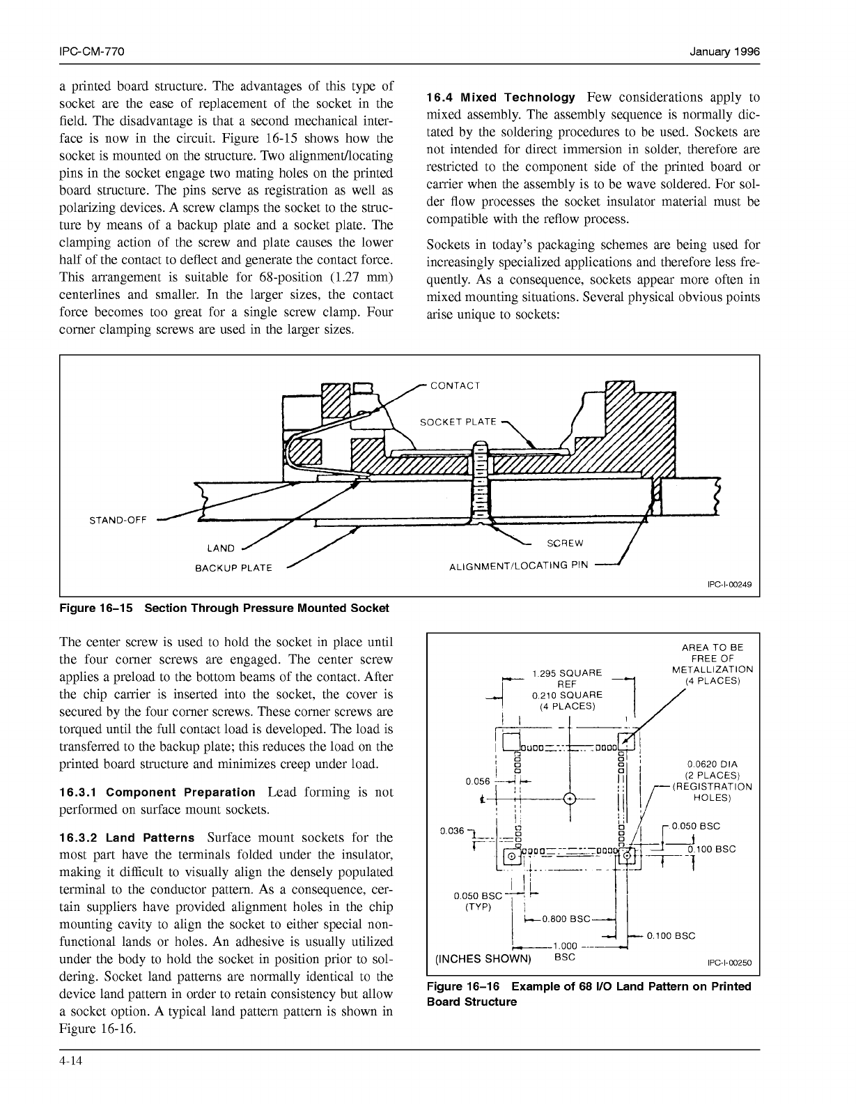
a printed board structure. The advantages of this type of
socket are the ease of replacement of the socket in the
16.4 Mixed Technology
Few considerations apply to
field. The disadvantage is that a second mechanical inter-
mixed assembly. The assembly sequence is normally dic-
face is now in the circuit. Figure 16-15 shows how the
tated by the soldering procedures to be used. Sockets are
socket is mounted on the structure. Two alignmendlocating
not intended for direct immersion in solder, therefore are
pins in the socket engage two mating holes on the printed
restricted to the component side of the printed board or
board
The
pins
Serve
as
registration
as
well
as
carrier when the assembly is to be wave soldered. For sol-
devices.
A
Screw clamps
the
socket
to
the
strut-
der flow processes the socket insulator material must be
ture by means of a backup plate and a socket plate. The
with
the
reflow
process.
clamping action of the Screw and Plate causes the lower Sockets in today's packaging schemes are being used for
half of the Contact to deflect and generate the Contact force. increasingly specialized applications and therefore less fre-
This arrangement is suitable for 68-Position
(1.27
mm> quently. As a consequence, sockets appear more often in
centerlines and smaller. In the larger sizes, the contact mixed mounting situations. Several physical obvious points
force becomes too great for a single screw clamp. Four arise unique to sockets:
comer clamping screws are used in the larger sizes.
STAND-OFF
SOCKET PLATE
BACKUP PLATE ALIGNMENT/LOCATING PIN
IPC-I
-00249
Figure 16-15 Section Through Pressure Mounted Socket
The center screw is used to hold the socket in place until
the four comer screws are engaged. The center screw
applies a preload to the bottom beams of the contact. After
the chip carrier is inserted into the socket, the cover is
secured by the four comer screws. These comer screws are
torqued until the full contact load is developed. The load is
transferred to the backup plate; this reduces the load on the
printed board structure and minimizes creep under load.
16.3.1 Component Preparation
Lead forming is not
performed on surface mount sockets.
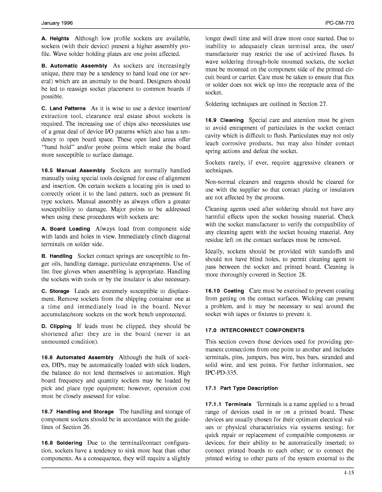
16.3.2 Land Patterns
Surface mount sockets for the
most part have the terminals folded under the insulator,
making it difficult to visually align the densely populated
terminal to the conductor pattern. As a consequence, cer-
tain suppliers have provided alignment holes in the chip
mounting cavity to align the socket to either special non-
functional lands or holes. An adhesive is usually utilized
under the body to hold the socket in position prior to sol-
dering. Socket land patterns are normally identical to the
device land pattern in order to retain consistency but allow
a socket option. A typical land pattern pattern is shown in
Figure 16- 16.
AREA TO BE
FREE OF
1
295 SQUARE
O
210
SQUARE
(4
PLACES)
METALLIZATION
REF
1
,(4
PLACES)
!Ll.OOO
---
(INCHES
SHOWN)
Esc IPC-I-O0250
Figure 16-16 Example
of
68
110
Land Pattern on Printed
Board Structure
4-14
COPYRIGHT Association Connecting Electronics Industries
Licensed by Information Handling Services
COPYRIGHT Association Connecting Electronics Industries
Licensed by Information Handling Services
January
1996
IPC-CM-770
A. Heights
Although low profile sockets are available,
sockets (with their device) present a higher assembly pro-
file. Wave solder holding plates are one point affected.
B. Automatic Assembly
As sockets are increasingly
unique, there may be a tendency to hand load one (or sev-
eral) which are an anomaly to the board. Designers should
be led to reassign socket placement to common boards if
possible.
C. Land Patterns
As it is wise to use a device insertion/
extraction tool, clearance real estate about sockets is
required. The increasing use of chips also necessitates use
of a great deal of device I/O patterns which also has a ten-
dency to open board space. These open land areas offer
“hand hold” and/or probe points which make the board
more susceptible to surface damage.
16.5 Manual Assembly
Sockets are normally handled
manually using special tools designed for ease of alignment
and insertion. On certain sockets a locating pin is used to
correctly orient it to the land pattern, such as pressure fit
type sockets. Manual assembly as always offers a greater
susceptibility to damage. Major points to be addressed
when using these procedures with sockets are:
A. Board Loading
Always load from component side
with lands and holes in view. Immediately clinch diagonal
terminals on solder side.
B. Handling
Socket contact springs are susceptible to fin-
ger oils, handling damage, particulate entrapments. Use of
lint free gloves when assembling is appropriate. Handling
the sockets with tools or by the insulator is also necessary.
C. Storage
Leads are extremely susceptible to displace-
ment. Remove sockets from the shipping container one at
a time and immediately load in the board. Never
accumulate/store sockets on the work bench unprotected.
D. Clipping
If
leads must be clipped, they should be
shortened after they are in the board (never in an
unmounted condition).
16.6 Automated Assembly
Although the bulk of sock-
ets, DIPS, may be automatically loaded with stick loaders,
the balance do not lend themselves to automation. High
board frequency and quantity sockets may be loaded by
pick and place type equipment; however, operation cost
must be closely assessed for value.
16.7 Handling and Storage
The handling and storage of
component sockets should be in accordance with the guide-
lines of Section
26.
16.8 Soldering
Due to the terminakontact configura-
tion, sockets have a tendency to sink more heat than other
components. As a consequence, they will require a slightly
longer dwell time and will draw more once started. Due to
inability to adequately clean terminal area, the user/
manufacturer may restrict the use of activized fluxes. In
wave soldering through-hole mounted sockets, the socket
must be mounted on the component side of the printed cir-
cuit board or carrier. Care must be taken to ensure that flux
or solder does not wick up into the receptacle area of the
socket.
Soldering techniques are outlined in Section
27.
16.9 Cleaning
Special care and attention must be given
to avoid entrapment of particulates in the socket contact
cavity which is difficult to flush. Particulates may not only
leach corrosive products, but may also hinder contact
spring actions and defeat the socket.
Sockets rarely, if ever, require aggressive cleaners or
techniques.
Non-normal cleaners and reagents should be cleared for
use with the supplier
so
that contact plating or insulators
are not affected by the process.
Cleaning agents used after soldering should not have any
harmful effects upon the socket housing material. Check
with the socket manufacturer to verify the compatibility of
any cleaning agent with the socket housing material. Any
residue left on the contact surfaces must be removed.
Ideally, sockets should be provided with standoffs and
should not have blind holes, to permit cleaning agent to
pass between the socket and printed board. Cleaning is
more thoroughly covered in Section
28.
16.1
O
Coating
Care must be exercised to prevent coating
from getting on the contact surfaces. Wicking can present
a problem, and it may be necessary to seal around the
socket with tapes or fixtures to prevent it.
17.0 INTERCONNECT COMPONENTS
This section covers those devices used for providing per-
manent connections from one point to another and includes
terminals, pins, jumpers, bus wire, bus bars, stranded and
solid wire, and test points. For further information, see
IPC-PD-335.
17.1 Part Type Description
17.1.1 Terminals
Terminals is a name applied to a broad
range of devices used in or on a printed board. These
devices are usually chosen for their optimum electrical val-
ues or physical characteristics via systems testing; for
quick repair or replacement of compatible components or
devices; for their ability to be automatically inserted; to
connect printed boards to each other; or to connect the
printed wiring to other parts of the system external to the
4-15
COPYRIGHT Association Connecting Electronics Industries
Licensed by Information Handling Services
COPYRIGHT Association Connecting Electronics Industries
Licensed by Information Handling Services
IPC-CM-770
Januaty
1996
printed boards. To provide mechanical strength to the ter- minal serves as the feed through device through the glass
minal and the resultant connection, most terminals are seal. See Figure
17-3.
designed for through-the-board mounting, either with
crimping, rolling, or flaring on the back side of the board,
or by an interference fit or “press fit” into the board.
Solder-only mounting may be used when the terminals are
only used as test points.
D.
Cup Terminals
cup terminals are not normally
attached to printed boards, but are often used as part of a
connection technique which does interface with a printed
board. Cup terminals are designed for either soldering (see
Figure
17-4)
or crimping (see Figure
17-5).
Terminals can be generally categorized as follows:
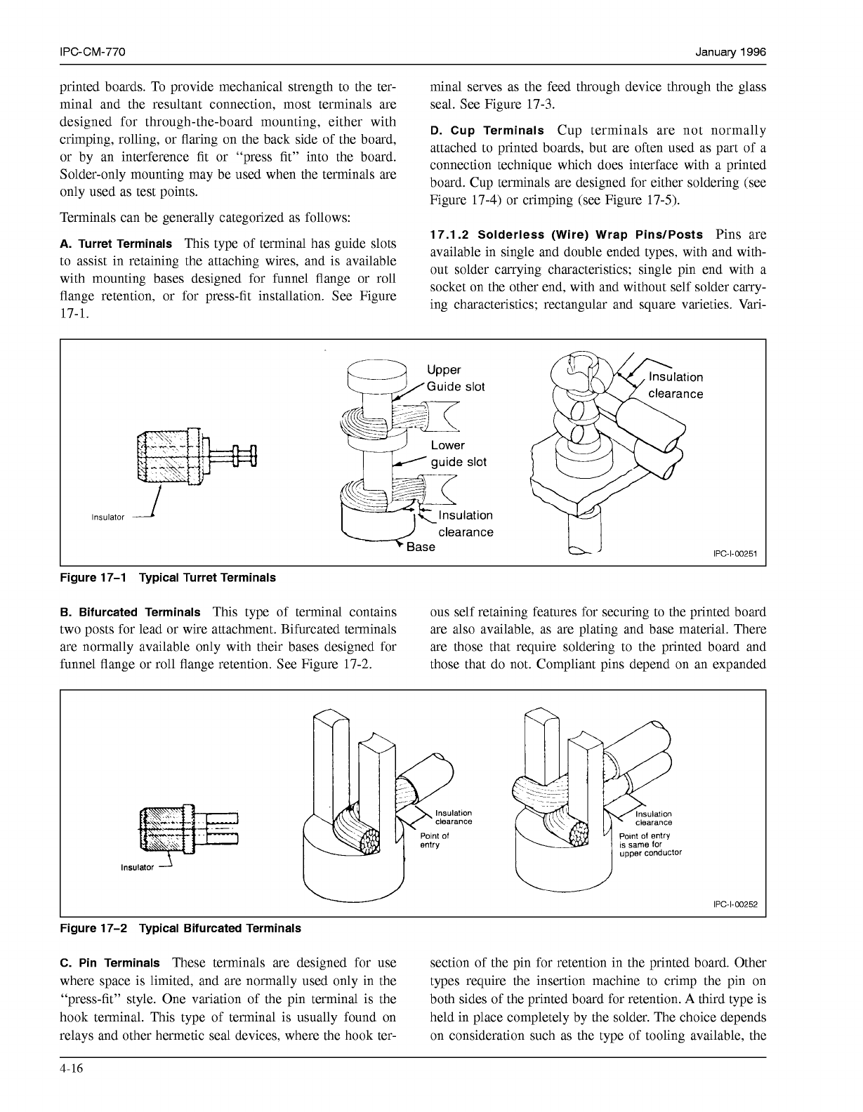
A.
Turret Terminals
This type of terminal has guide slots
to assist in retaining the attaching wires, and is available
with mounting bases designed for funnel flange or roll
flange retention, or for press-fit installation. See Figure
17.1.2 Solderless (Wire) Wrap PinslPosts
Pins are
available in single and double ended types, with and with-
out solder carrying characteristics; single pin end with a
socket on the other end, with and without self solder carry-
ing characteristics; rectangular and square varieties. Vari-
17-1.
I
guide
slot
dase
clearance
IPC-I-O0251
Figure 17-1 Typical Turret Terminals
B. Bifurcated Terminals
This type of terminal contains ous self retaining features for securing to the printed board
two posts for lead or wire attachment. Bifurcated terminals are also available, as are plating and base material. There
are normally available only with their bases designed for are those that require soldering to the printed board and
funnel flange or roll flange retention. See Figure
17-2.
those that do not. Compliant pins depend on an expanded
lnsulatlon
clearance
Polnt
o1
entry
IS
same for
upper conductor
IPC-I-O0252
Figure 17-2 Typical Bifurcated Terminals
C. Pin Terminals
These terminals are designed for use section of the pin for retention in the printed board. Other
where space is limited, and are normally used only in the types require the insertion machine to crimp the pin on
“press-fit’’ style. One variation of the pin terminal is the both sides of the printed board for retention.
A
third type is
hook terminal. This type of terminal is usually found on held in place completely by the solder. The choice depends
relays and other hermetic seal devices, where the hook ter- on consideration such as the type of tooling available, the
4-16
COPYRIGHT Association Connecting Electronics Industries
Licensed by Information Handling Services
COPYRIGHT Association Connecting Electronics Industries
Licensed by Information Handling Services