IPC-CM-770D-1996 - 第89页
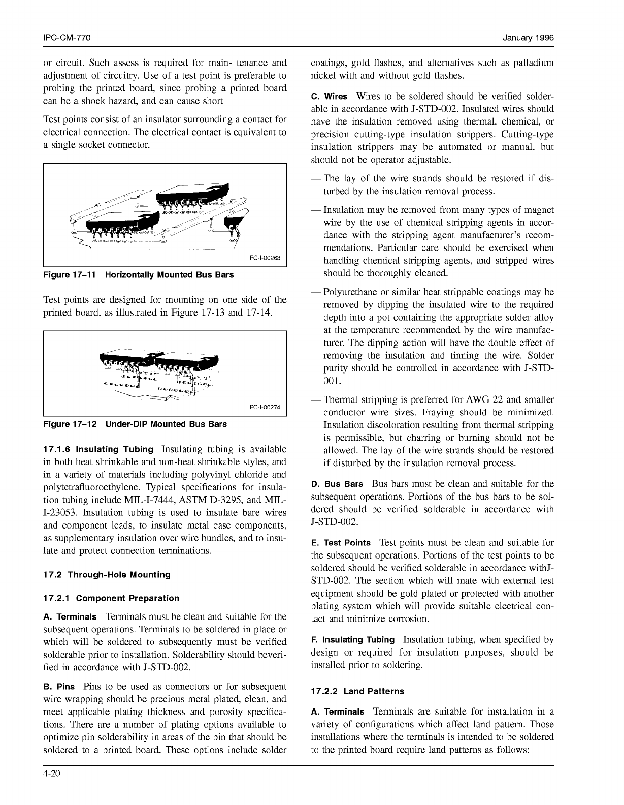
January 1996 IPC-CM-770 Hardware Mount Solder Mount IPC-1-00265 Figure 17-13 One-terminal Printed Board Test Point IPC-1-00266 Figure 17-1 4 Two-terminal Printed Board Test Point Single Sided Board, Soldered on Shoulder …
IPC-CM-770
Januaty
1996
or circuit. Such assess is required for main- tenance and
adjustment of circuitry. Use of a test point is preferable to
probing the printed board, since probing a printed board
can be a shock hazard, and can cause short
Test points consist of an insulator surrounding a contact for
electrical connection. The electrical contact is equivalent to
a single socket connector.
I
IPC-1-00263
I
Figure 17-11 Horizontally Mounted Bus Bars
Test points are designed for mounting on one side of the
printed board, as illustrated in Figure 17-13 and 17-14.
IPC-1-00274
Figure 17-12 Under-DIP Mounted Bus Bars
17.1.6 Insulating Tubing
Insulating tubing is available
in both heat shrinkable and non-heat shrinkable styles, and
in a variety of materials including polyvinyl chloride and
polytetrafluoroethylene.
Typical specifications for insula-
tion tubing include MIL-1-7444, ASTM D-3295, and MIL-
1-23053. Insulation tubing is used to insulate bare wires
and component leads, to insulate metal case components,
as supplementary insulation over wire bundles, and to insu-
late and protect connection terminations.
17.2 Through-Hole Mounting
17.2.1 Component Preparation
A.
Terminals
Terminals must be clean and suitable for the
subsequent operations. Terminals to be soldered in place or
which will be soldered to subsequently must be verified
solderable prior to installation. Solderability should beveri-
fied in accordance with J-STD-002.
B. Pins
Pins to be used as connectors or for subsequent
wire wrapping should be precious metal plated, clean, and
meet applicable plating thickness and porosity specifica-
tions. There are a number of plating options available to
optimize pin solderability in areas of the pin that should be
soldered to a printed board. These options include solder
coatings, gold flashes, and alternatives such as palladium
nickel with and without gold flashes.
C. Wires
Wires to be soldered should be verified solder-
able in accordance with J-STD-002. Insulated wires should
have the insulation removed using thermal, chemical, or
precision cutting-type insulation strippers. Cutting-type
insulation strippers may be automated or manual, but
should not be operator adjustable.
-The lay of the wire strands should be restored if dis-
turbed by the insulation removal process.
-
Insulation may be removed from many types of magnet
wire by the use of chemical stripping agents in accor-
dance with the stripping agent manufacturer's recom-
mendations. Particular care should be exercised when
handling chemical stripping agents, and stripped wires
should be thoroughly cleaned.
-
Polyurethane or similar heat strippable coatings may be
removed by dipping the insulated wire to the required
depth into a pot containing the appropriate solder alloy
at the temperature recommended by the wire manufac-
turer. The dipping action will have the double effect of
removing the insulation and tinning the wire. Solder
purity should be controlled in accordance with J-STD-
001.
-
Thermal stripping is preferred for AWG 22 and smaller
conductor wire sizes. Fraying should be minimized.
Insulation discoloration resulting from thermal stripping
is permissible, but charring or burning should not be
allowed. The lay of the wire strands should be restored
if disturbed by the insulation removal process.
D. Bus Bars
Bus bars must be clean and suitable for the
subsequent operations. Portions of the bus bars to be sol-
dered should be verified solderable in accordance with
J-STD-002.
E.
Test Points
Test points must be clean and suitable for
the subsequent operations. Portions of the test points to be
soldered should be verified solderable in accordance withJ-
STD-002. The section which will mate with external test
equipment should be gold plated or protected with another
plating system which will provide suitable electrical con-
tact and minimize corrosion.
F. Insulating Tubing
Insulation tubing, when specified by
design or required for insulation purposes, should be
installed prior to soldering.
17.2.2 Land Patterns
A.
Terminals
Terminals are suitable for installation in a
variety of configurations which affect land pattern. Those
installations where the terminals is intended to be soldered
to the printed board require land patterns as follows:
4-20
COPYRIGHT Association Connecting Electronics Industries
Licensed by Information Handling Services
COPYRIGHT Association Connecting Electronics Industries
Licensed by Information Handling Services
January
1996
IPC-CM-770
Hardware Mount
Solder Mount
IPC-1-00265
Figure 17-13 One-terminal Printed Board Test Point
IPC-1-00266
Figure 17-1
4
Two-terminal Printed Board Test Point
Single Sided Board, Soldered on Shoulder Side.
The land
pattern should be a minimum of
0.5
mm larger in diam-
eter than the diameter of the terminal shoulder. The clear-
ance between the terminal shank and the hole should be
0.13
mm maximum. See Figure
17-15.
Single Sided Board, Soldered on Flange Side.
The land
pattern should be a minimum of
0.5
mm larger in diam-
eter than the projection of the flared flange. The difference
idiameter between the terminal shank and the hole should
be
0.13
mm maximum. See Figure
17-16.
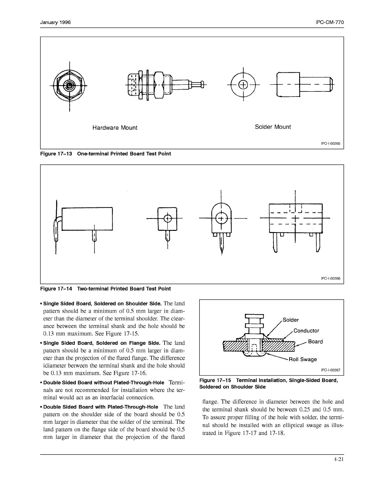
Double Sided Board without Plated-Through-Hole
Termi-
nals are not recommended for installation where the ter-
minal would act as an interfacial connection.
Double Sided Board with Plated-Through-Hole
The land
pattern on the shoulder side of the board should be
0.5
mm larger in diameter that the solder of the terminal. The
land pattern on the flange side of the board should be
0.5
mm larger in diameter that the projection of the flared
I
IPC-1-00267
Figure 17-15 Terminal Installation, Single-Sided Board,
Soldered on Shoulder Side
flange. The difference in diameter between the hole and
the terminal shank should be between
0.25
and
0.5
mm.
To assure proper filling of the hole with solder, the termi-
nal should be installed with an elliptical swage as illus-
trated in Figure
17-17
and
17-18.
4-21
COPYRIGHT Association Connecting Electronics Industries
Licensed by Information Handling Services
COPYRIGHT Association Connecting Electronics Industries
Licensed by Information Handling Services
IPC-CM-770
Januaty
1996
I
IPC-1-00268
I
Figure 17-1
6
Terminal Installation, Single-Sided Board,
Soldered on Flared Flange Side
IPC-1-00269
I
L
Figure 17-17 Installation of Terminal in Plated-through
Hole
r-""
30"160"
swaging
tool
r--
-
"1
I
\
\"",I
on swagmg
tool
Grind or.mlll flats
I
Plated-thru
hole
IPC-I-O0270
L
Figure 17-1
8
Elliptical Swaging
B. Pins
Pins should be soldered in plated-through-holes,
and the standard requirements for minimum annular ring
(0.13
mm minimum) apply.
C. Wires
Wires, when soldered to printed boards, utilize
the same land configurations as through-the-board mounted
components.
D. Bus Bars
Bus bars utilize the same land configurations
as through-the-board mounted components.
E. Test Points
Test points utilize the same land configu-
ration as through-the-board mounted components.
17.2.3 Lead Configuration After Assembly
17.2.3.1 Soldered Assemblies
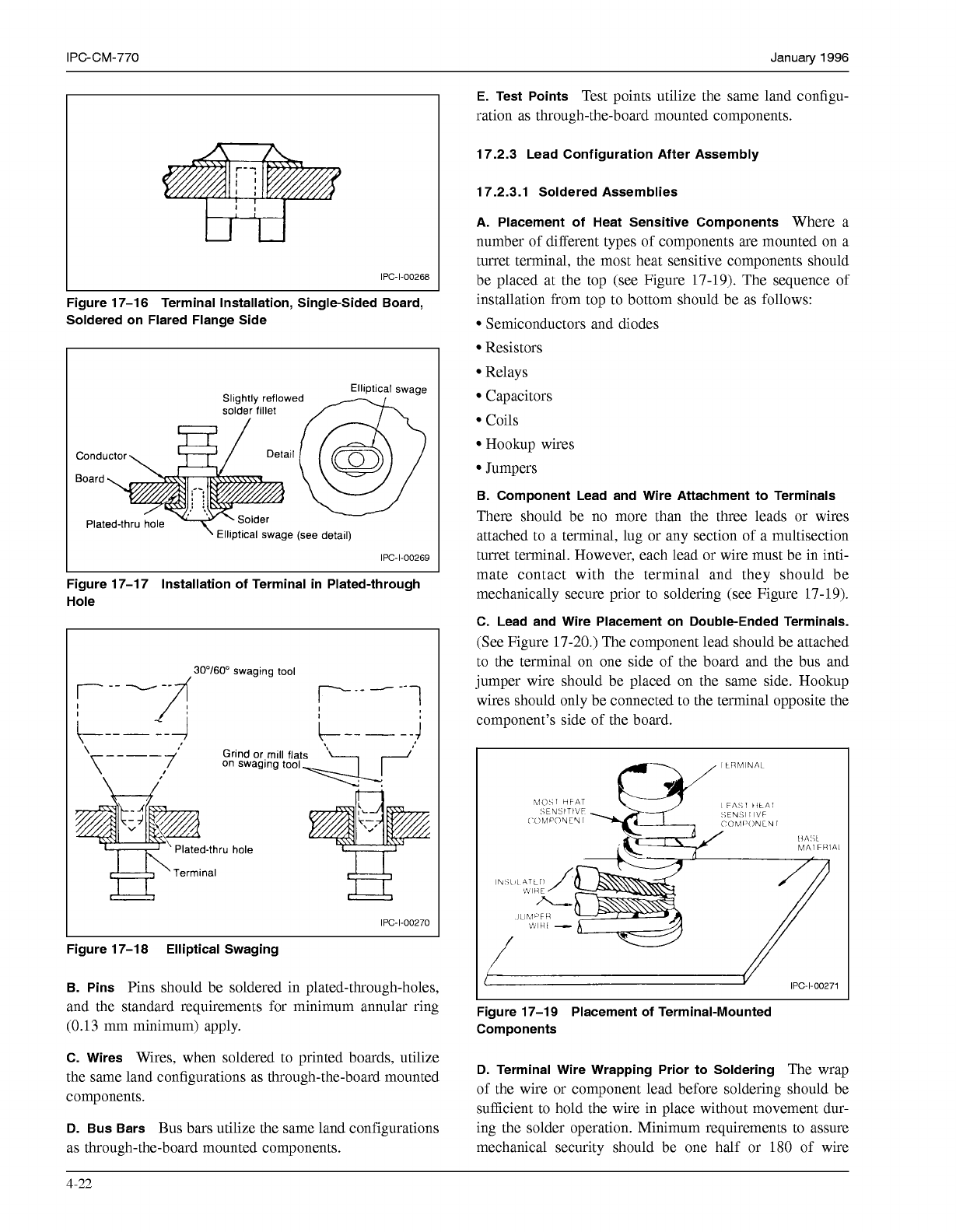
A. Placement of Heat Sensitive Components
Where a
number of different types of components are mounted on a
turret terminal, the most heat sensitive components should
be placed at the top (see Figure 17-19). The sequence of
installation from top to bottom should be as follows:
Semiconductors and diodes
Resistors
Relays
Capacitors
Coils
Hookup wires
Jumpers
B. Component Lead and Wire Attachment to Terminals
There should be no more than the three leads or wires
attached to a terminal, lug or any section of a multisection
turret terminal. However, each lead or wire must be in inti-
mate contact with the terminal and they should be
mechanically secure prior to soldering (see Figure 17-19).
C. Lead and Wire Placement on Double-Ended Terminals.
(See Figure 17-20.) The component lead should be attached
to the terminal on one side of the board and the bus and
jumper wire should be placed on the same side. Hookup
wires should only be connected to the terminal opposite the
component's side of the board.
V
IPC-I-O0271
Figure 17-19 Placement of Terminal-Mounted
Components
D. Terminal Wire Wrapping Prior to Soldering
The wrap
of the wire or component lead before soldering should be
sufficient to hold the wire in place without movement dur-
ing the solder operation. Minimum requirements to assure
mechanical security should be one half or
180
of wire
4-22
COPYRIGHT Association Connecting Electronics Industries
Licensed by Information Handling Services
COPYRIGHT Association Connecting Electronics Industries
Licensed by Information Handling Services