IPC 7711A.pdf - 第212页
CAUTION Exercise care to prevent bubbles in the epoxy mixture. 5. Pour the epoxy into the epoxy cartridge. 6. Inject the epoxy into one of the holes in the delamination. (See Figure 2.) The heat retained in the printed w…
OUTLINE
This method is used to repair mechanical or thermal blisters or delaminations in
printed wiring board laminated base materials. The blister is sealed by injecting a low
viscosity epoxy into the blister/delamination void.
CAUTION
This method can only be used when the laminate base material has separated suf-
ficiently to allow the epoxy to flow throughout the void area.
REFERENCES
2.1 Handling Electronic Assemblies
2.2 Cleaning
2.5 Baking and Preheating
2.6 Epoxy Mixing and Handling
TOOLS & MATERIALS
Ball Mill, #1/2
Cleaner
Cleaning Wipes
Epoxy
Epoxy Cartridge with Tip
Epoxy Injection System, Optional
Hand Held Drill
Heat Lamp
Oven
Scraper
Vacuum Source, Optional
PROCEDURE
1. Clean the area.
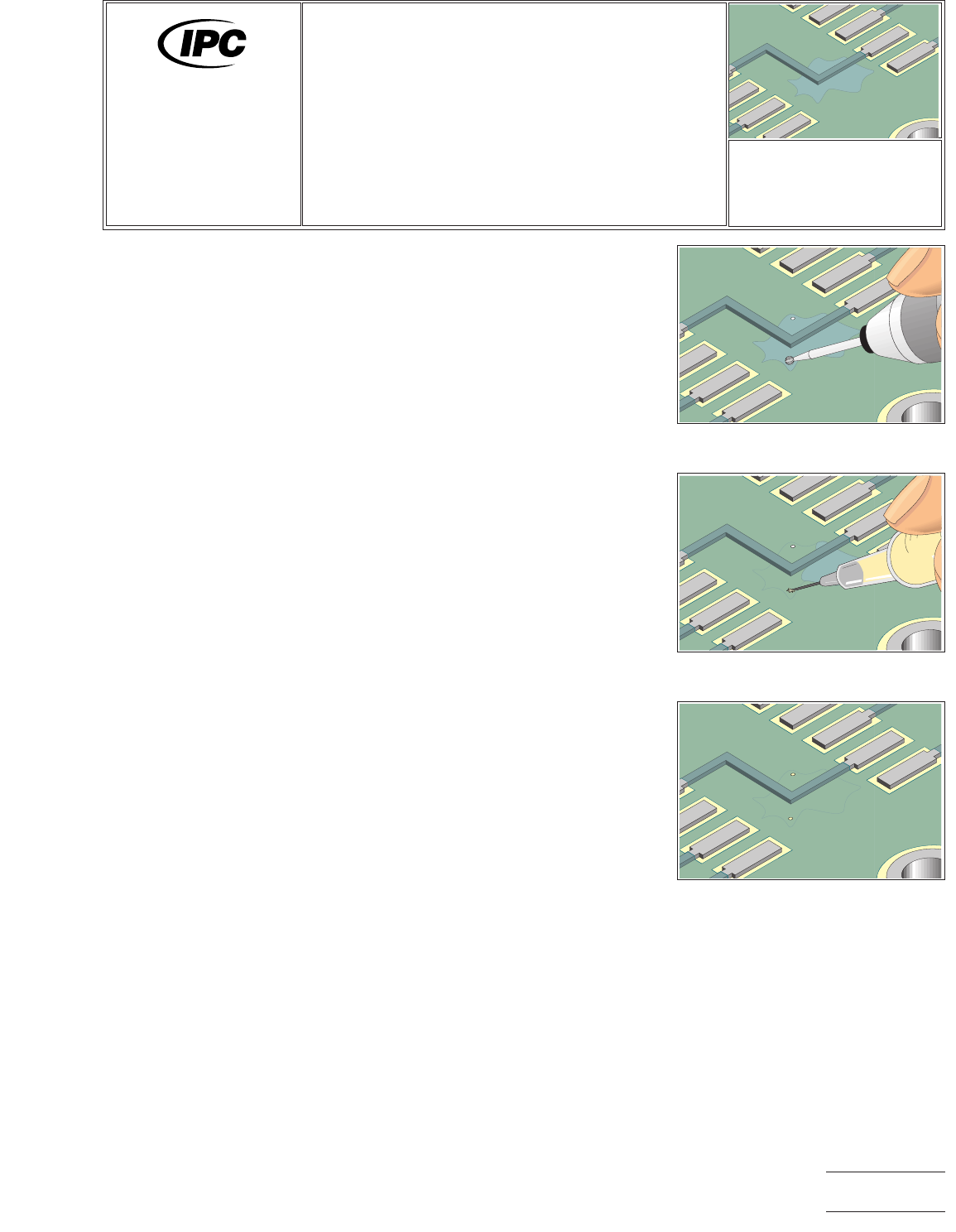
2. Drill into delamination blister with the dental style drill and ball mill. Drill in an area
clear of circuitry or components. Drill at least two holes opposite each other
around the perimeter of the delamination. (See Figure 1.) Brush away all loose
material.
CAUTION
Be careful not to drill too deep exposing internal conductors or planes.
CAUTION
Abrasion operations can generate electrostatic charges.
3. Bake the printed wiring board to remove any entrapped moisture. Do not allow
the printed wiring board to cool prior to injecting the epoxy.
CAUTION
Some components may be sensitive to high temperature.
4. Mix the epoxy. See manufacturers instructions on how to mix epoxy without
bubbles.
Figure 1 Drill into the delamination
blister
Figure 2 Inject epoxy into the
delamination blister.
Figure 3 Completed Repair.
7721A
Repair and
Modification of
Printed Boards and
Electronic Assemblies
Revision:
Date: 2/98
Delamination/Blister
Repair, Injection Method
Number: 3.1
Product Class: R
Skill Level: Advanced
Level of Conformance: High
Material in this manual was voluntarily established by Technical Committees of IPC. This material is advisory only and its use
or adaptation is entirely voluntary. IPC disclaims all liability of any kind as to the use, application, or adaptation of this material.
Users are also wholly responsible for protecting themselves against all claims or liabilities for patent infringement. Equipment
referenced is for the convenience of the user and does not imply endorsement by IPC.
Page1of2
Copyright Association Connecting Electronics Industries
Provided by IHS under license with IPC
Not for Resale
No reproduction or networking permitted without license from IHS
--``,``,-`-`,,`,,`,`,,`---

CAUTION
Exercise care to prevent bubbles in the epoxy mixture.
5. Pour the epoxy into the epoxy cartridge.
6. Inject the epoxy into one of the holes in the delamination. (See Figure 2.) The heat
retained in the printed wiring board will improve the flow characteristics of the
epoxy and will draw the epoxy into the void area filling it completely.
7. If the void does not fill completely, the following procedures may be used:
A. Apply light local pressure on the board surface starting at the fill hole, slowly
proceeding to the vent hole.
B. Apply vacuum to the vent hole to draw the epoxy through the void.
8. Cure the epoxy per the manufacturers recommendation.
9. Scrape away any excess epoxy using a knife or scraper.
NOTE
If needed, apply additional thin coating to seal any scrapped areas.
EVALUATION
1. Visual examination for texture and color match.
2. Electrical tests to conductors around the repaired area as applicable.
NOTES
IPC-7721A
Number: 3.1
Revision:
Date: 2/98
Subject: Delamination/Blister Repair, Injection Method
Page2of2
Copyright Association Connecting Electronics Industries
Provided by IHS under license with IPC
Not for Resale
No reproduction or networking permitted without license from IHS
--``,``,-`-`,,`,,`,`,,`---
OUTLINE
This method is used to eliminate, or reduce the bow and twist, or warping of printed
wiring boards. The warping is removed by controlled heating and cooling of the
printed wiring board while under restraint.
CAUTION
This repair method is most suitable for FR-4, GE or GF substrate base materials
having glass transition temperatures below 125°C. The bake/time cycle will have to
be adjusted depending on the base material glass transistion temperature.
CAUTION
This process uses high temperatures. Some components may be sensitive to high
temperature and should be removed if this procedure will adversely affect them.
CAUTION
High temperatures will cause oxidation of solderable surfaces.
NOTE
Bow and twist should not be repaired unless sited as a defect.
REFERENCES
2.1 Handling Electronic Assemblies
2.5 Baking and Preheating
TOOLS & MATERIALS
Base Plate
Caliper or Pin Gauges
Oven
Restraint Bars
Restraint Clamps
PROCEDURE
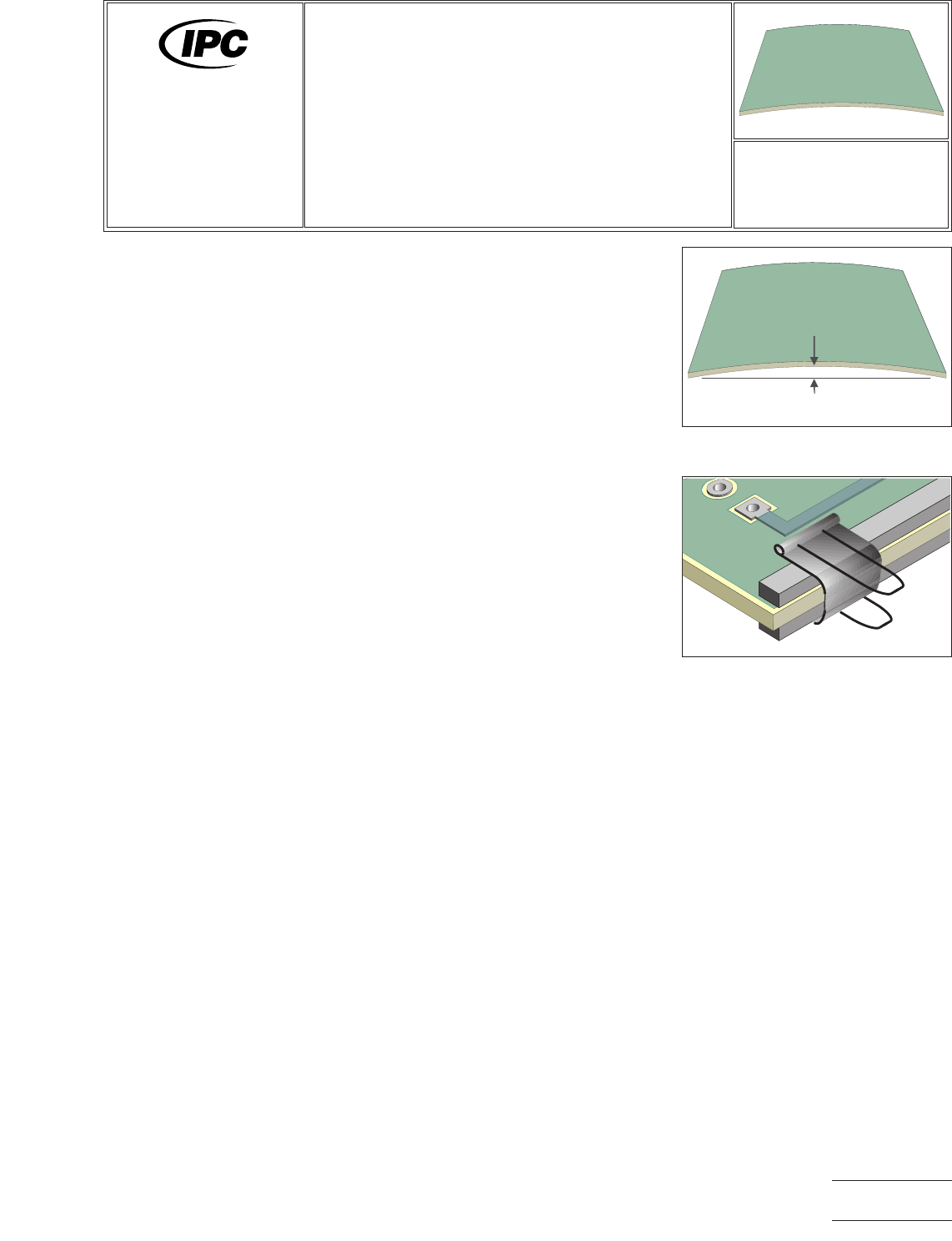
1. Check the deflection to determine if rework is needed. (See Figure 1.)
NOTE
Bow and twist after soldering shall not exceed 1.5% for through-hole printed wir-
ing boards and 0.75% for surface mount printed wiring boards. The bow and
twist shall not be sufficient to cause difficulties during placement, soldering and
testing operations. Before dispositioning printed wiring boards with bow and twist
as scrap, keep in mind how the printed wiring board is mounted in it’s final des-
tination. Keep in mind ‘‘form, fit and function’’ without jeopardizing reliability.
2. Place the restraint bars along the edges that require rework. (See Figure 2.)
CAUTION
Components or parts that will interfere with the restraint bars should be removed.
Figure 1 Check edge deflection for
maximum wrap.
Figure 2 Clamp restraint bars to edge
needing rework.
7721A
Repair and
Modification of
Printed Boards and
Electronic Assemblies
Revision:
Date: 2/98
Bow and Twist Repair
Number: 3.2
Product Class: R, W
Skill Level: Advanced
Level of Conformance: Medium
Material in this manual was voluntarily established by Technical Committees of IPC. This material is advisory only and its use
or adaptation is entirely voluntary. IPC disclaims all liability of any kind as to the use, application, or adaptation of this material.
Users are also wholly responsible for protecting themselves against all claims or liabilities for patent infringement. Equipment
referenced is for the convenience of the user and does not imply endorsement by IPC.
Page1of2
Copyright Association Connecting Electronics Industries
Provided by IHS under license with IPC
Not for Resale
No reproduction or networking permitted without license from IHS
--``,``,-`-`,,`,,`,`,,`---