IPC 7711A.pdf - 第244页
7. Select a wire to match the width and thickness of the conductor to be replaced. Cut a length approximately as needed. See Table 1 for Solid Wire Equivalents. 8. Strip the wire and tin the ends if needed. Non-insulated…
OUTLINE
This method is used on printed wiring boards to replace damaged or missing con-
ductors on the printed wiring board surface. A length of standard insulated or non-
insulated wire is used to repair the damaged conductor.
CAUTION
The conductor widths, spacing and current carrying capacity must not be reduced
below allowable tolerances.
REFERENCES
2.1 Handling Electronic Assemblies
2.2 Cleaning
2.5 Baking and Preheating
TOOLS AND MATERIALS
Cleaner
Cleaning Wipes
Epoxy
Heat Lamp
Polyimide Tape
Knife
Light
Liquid Flux
Microscope
Oven
Scraper
Solder
Soldering Iron with Tips
Wire
Wire Guide Tool
PROCEDURE
1. Clean the area.
2. Remove the damaged section of conductor using a knife. The damaged con-
ductor should be trimmed back to a point where the conductor still has a good
bond to the printed wiring board surface.
NOTE
Heat can be applied to the damaged conductor using a soldering iron to allow
the conductor to be removed more easily.
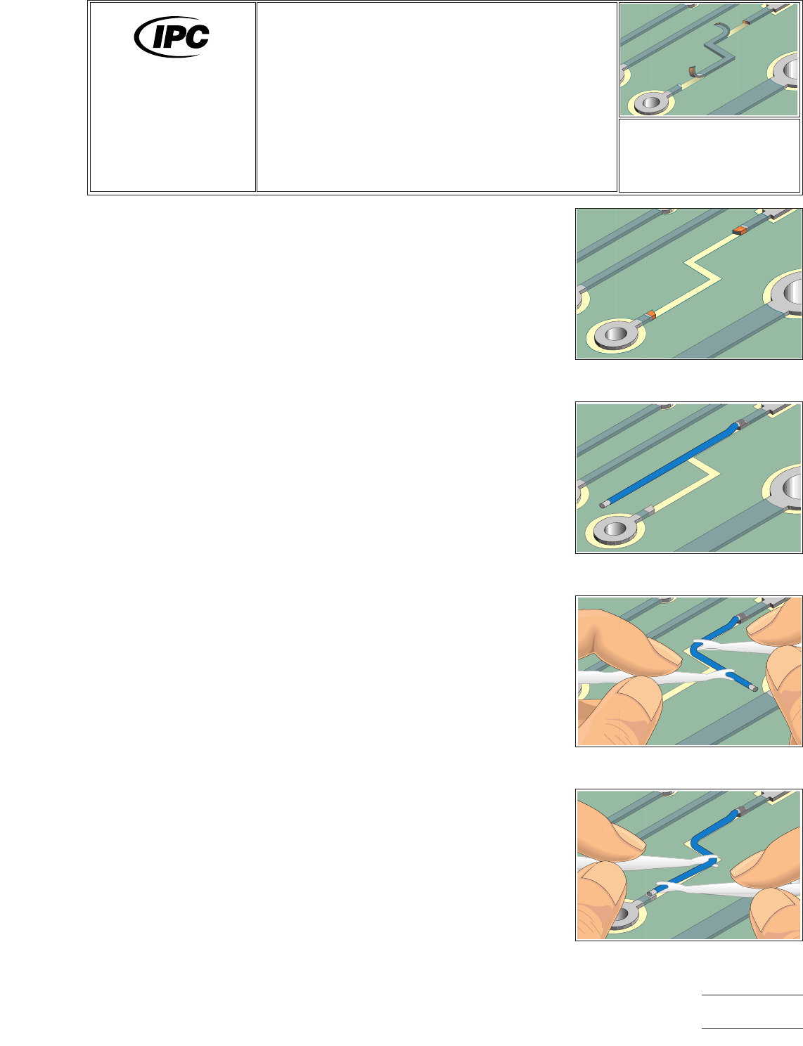
3. Use a knife and scrape off any solder resist or coating from the ends of the
remaining conductor. (See Figure 1.)
4. Remove all loose material. Clean the area.
5. Apply a small amount of liquid flux to the ends of the remaining conductor. Tin
the exposed end of each conductor using solder and a soldering iron.
6. Clean the area.
Figure 1 Scrap off any coating from
the ends of the conductors.
Figure 2 Lap solder the wire to one
end of the conductor.
Figure 3 Form wire using wire guide
tools.
Figure 4 Form the final shape of the
wire and solder in place.
7721A
Repair and
Modification of
Printed Boards and
Electronic Assemblies
Revision:
Date: 2/98
Conductor Repair,
Surface Wire Method
Number: 4.2.4
Product Class: R, F, C
Skill Level: Intermediate
Level of Conformance: Medium
Material in this manual was voluntarily established by Technical Committees of IPC. This material is advisory only and its use
or adaptation is entirely voluntary. IPC disclaims all liability of any kind as to the use, application, or adaptation of this material.
Users are also wholly responsible for protecting themselves against all claims or liabilities for patent infringement. Equipment
referenced is for the convenience of the user and does not imply endorsement by IPC.
Page1of4
Copyright Association Connecting Electronics Industries
Provided by IHS under license with IPC
Not for Resale
No reproduction or networking permitted without license from IHS
--``,``,-`-`,,`,,`,`,,`---
7. Select a wire to match the width and thickness of the conductor to be replaced.
Cut a length approximately as needed. See Table 1 for Solid Wire Equivalents.
8. Strip the wire and tin the ends if needed. Non-insulated wire may be used for
short repairs if conductors are not crossed.
9. Clean the wire.
10. If the wire is long or has bends, one end may be soldered prior to forming the
new shape. Place the wire in position. The wire should overlap the existing con-
ductor a minimum of 2 times the conductor width. The wire may be held in
place with Polyimide tape during soldering.
NOTE
If the configuration permits, the overlap solder joint connection should be a
minimum of 3.00 mm from the related termination. This gap will minimize the
possibility of simultaneous reflow during soldering operations. Refer to 7.1 Sol-
dering Basics.
11. Apply a small amount of liquid flux to the overlap joint.
12. Lap solder the wire to one end of the conductor on the printed wiring board
surface. Make sure the wire is properly aligned. (See Figure 2.)
13. Bend the wire as needed to match the shape of the missing conductor. (See
Figure 3.)
NOTE
Wire guide tools can be used to form the wire as needed.
14. Lap solder the other wire end to the remaining conductor on the printed wiring
board surface using solder and a soldering iron. Make sure the wire is properly
aligned. (See Figure 4.)
15. Remove any Polyimide tape and clean the area.
NOTE
It may be necessary to encapsulate the solder joint connection if electrical spac-
ing is reduced or the connection is beneath a component.
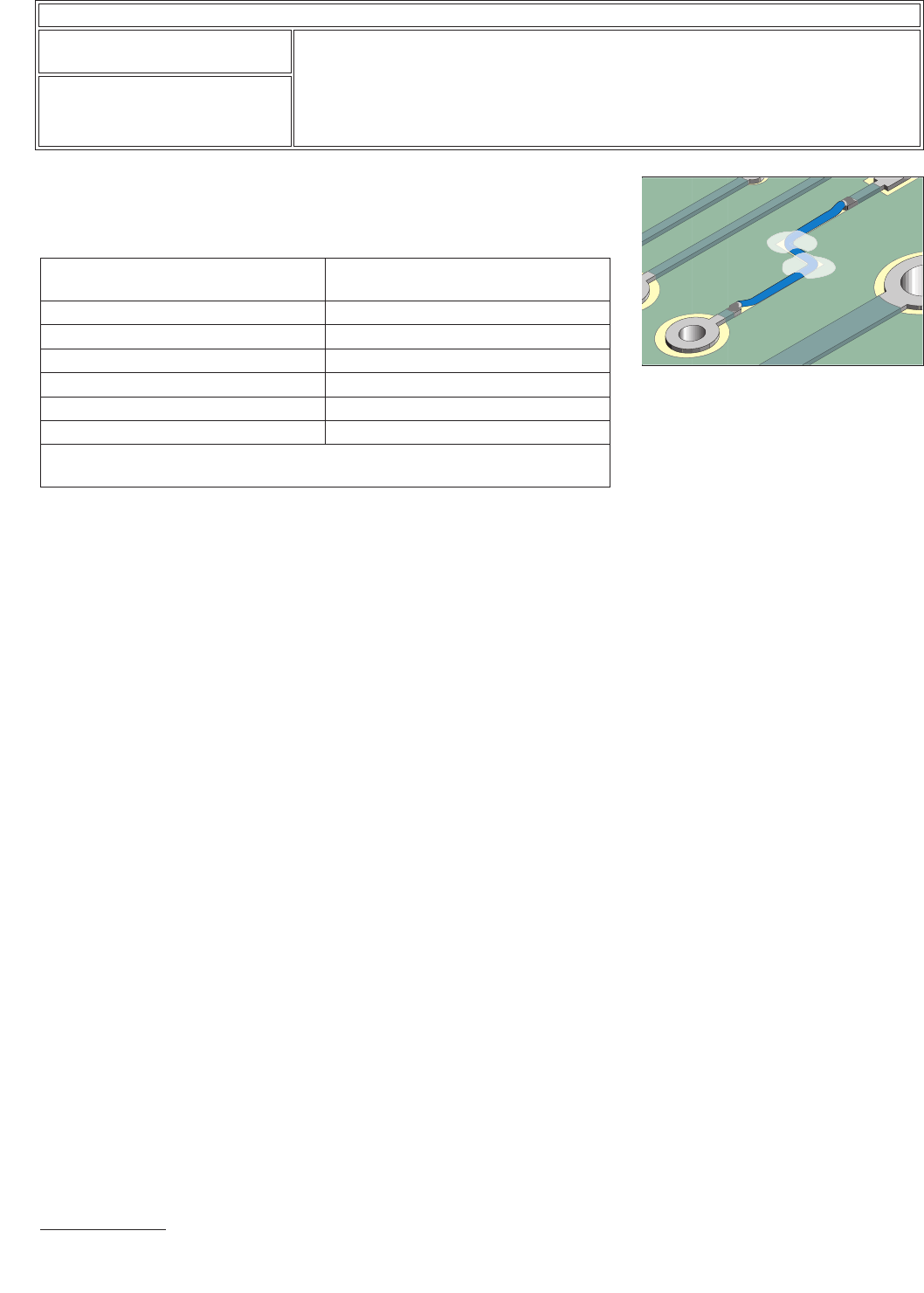
16. If desired bond the wire to the printed wiring board surface with adhesive, epoxy
or tape dots. (See Figure 5.)
Figure 5 Bond the wire to the surface
with adhesive or tape.
Table 1 Solid Wire Equivalents
Conductor Width
2 oz. Copper
Equivalent Solid
Wire Diameter
0.25 mm #34, 0.15 mm
0.38 mm #32, 0.20 mm
0.50 mm #31, 0.23 mm
0.78 mm #29, 0.28 mm
2.08 mm #26, 0.46 mm
3.18 mm #23, 0.58 mm
When using solid wire to repair a conductor, there should be no reduction in the
cross sectional area.
IPC-7721A
Number: 4.2.4
Revision:
Date: 2/98
Subject: Conductor Repair, Surface Wire Method
Page2of4
Copyright Association Connecting Electronics Industries
Provided by IHS under license with IPC
Not for Resale
No reproduction or networking permitted without license from IHS
--``,``,-`-`,,`,,`,`,,`---

CAUTION
Some components may be sensitive to high temperature.
17. Cure the epoxy per the manufacturers instructions.
18. After the epoxy has cured clean the area.
EVALUATION
1. Visual examination for alignment and overlap of wire.
2. Electrical tests as applicable.
IPC-7721A
Number: 4.2.4
Revision:
Date: 2/98
Subject: Conductor Repair, Surface Wire Method
Page3of4
Copyright Association Connecting Electronics Industries
Provided by IHS under license with IPC
Not for Resale
No reproduction or networking permitted without license from IHS
--``,``,-`-`,,`,,`,`,,`---