IPC 7711A.pdf - 第255页
15. Coat the top and sides of the replaced conductor with epoxy. The epoxy bonds the new conductor to the base board material and insulates the conductor. Continue adding epoxy up to the top surface of the printed wiring…
3. Use the microscope and hand held drill and cut through the base material, one
layer at a time, until the desired inner layer has been reached. (See Figure 1 and
2.)
CAUTION
Great care should be taken to prevent further damage to internal conductors.
4. Each internal conductor should have a flat section exposed to allow the new
conductor to be soldered in place. (See Figure 3.)
NOTE
To reduce damage to the internal conductor, complete the final exposure of the
internal conductor using a knife. (See Figure 3.)
5. Remove all loose material. Clean the area.
6. Apply a small amount of liquid flux to the ends of the internal conductor. Tin the
exposed end of each conductor using solder and a soldering iron.
7. Clean the area.
8. Select a replacement conductor foil jumper that most closely matches the size
of the conductor to be replaced. Cut length approximately as needed.
9. Gently abrade the top and bottom of the conductor foil jumper with a buffer to
remove any protective coating and clean.
NOTE
If needed, the ends of the conductor foil jumper may be tinned with solder prior
to lap soldering in place.
10. Place the conductor foil jumper in position. The conductor foil jumper should
overlap the existing conductor a minimum of 2 times the conductor width. (See
Figure 4.)
NOTE
If spacing is critical or the printed wiring board uses high frequency conductors,
bevel the joint. (See Figure 5.)
CAUTION
This bevel joint method may cause problems with printed wiring boards
exposed to extreme temperature fluctuations.
11. Apply a small amount of liquid flux to the overlap joint.
12. Lap solder the conductor foil jumper to the exposed internal conductor using
solder and a soldering iron. Make sure the new conductor is properly aligned.
13. Clean the area.
NOTE
The printed wiring board may be preheated prior to filling the area with epoxy.
A preheated printed wiring board will allow the epoxy to easily flow and level out.
Epoxy applied to an unheated printed wiring board may settle below the printed
wiring board surface as the epoxy cures.
14. Mix epoxy. If desired, add color agent to the mixed epoxy to match the printed
wiring board color.
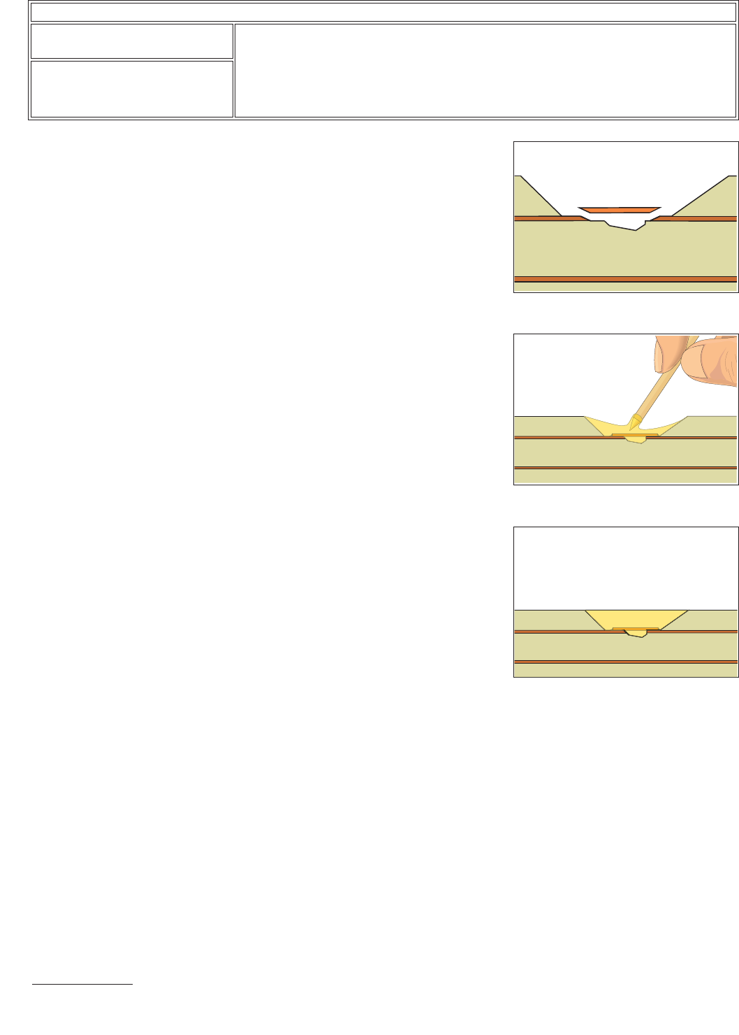
Figure 5 Bevel end joint.
Figure 6 Coat the top and sides of the
new conductor with epoxy.
Figure 7 Completed repair.
IPC-7721A
Number: 4.2.7
Revision:
Date: 2/98
Subject: Conductor Repair, Inner Layer Method
Page2of4
Copyright Association Connecting Electronics Industries
Provided by IHS under license with IPC
Not for Resale
No reproduction or networking permitted without license from IHS
--``,``,-`-`,,`,,`,`,,`---

15. Coat the top and sides of the replaced conductor with epoxy. The epoxy bonds
the new conductor to the base board material and insulates the conductor.
Continue adding epoxy up to the top surface of the printed wiring board or to
the height of the next internal conductor. (See Figure 6.)
NOTE
A slight overfill of epoxy may be desired to allow for shrinkage when the epoxy
cures.
16. Cure the epoxy per the manufacturer’s instructions.
CAUTION
Some components may be sensitive to high temperature.
17. Add additional conductor foil jumpers if needed and coat with additional epoxy.
18. Continue completing all layers until the top surface of the printed wiring board is
reached. (See Figure 7.)
19. Clean the board as required.
20. Apply surface coating to match prior coating as required.
EVALUATION
1. Visual examination for alignment and overlap of new conductor.
2. Visual examination of epoxy coating for texture and color match.
3. Electrical tests as applicable.
IPC-7721A
Number: 4.2.7
Revision:
Date: 2/98
Subject: Conductor Repair, Inner Layer Method
Page3of4
Copyright Association Connecting Electronics Industries
Provided by IHS under license with IPC
Not for Resale
No reproduction or networking permitted without license from IHS
--``,``,-`-`,,`,,`,`,,`---

NOTES
IPC-7721A
Number: 4.2.7
Revision:
Date: 2/98
Subject: Conductor Repair, Inner Layer Method
Page4of4
Copyright Association Connecting Electronics Industries
Provided by IHS under license with IPC
Not for Resale
No reproduction or networking permitted without license from IHS
--``,``,-`-`,,`,,`,`,,`---