IPC 7711A.pdf - 第270页
3. Use the knife and scrape off any epoxy residue, contamination or burned mate- rial from the board surface. CAUTION Abrasion operations can generate electrostatic charges. 4. Scrape off any solder resist or coating fro…
OUTLINE
This method is used to replace damaged and lifted lands. The damaged lands are
replaced with new lands. The new lands are bonded to the printed wiring board sur-
face using a commercially available epoxy.
CAUTION
This method is used to replace a damaged or missing land, but the new land will not
have an intermetallic connection to the remaining plated hole. The solder joint of the
replaced component will restore the electrical connection. If a component is not
installed, a wire clinched to both sides of the printed wiring board may be used.
CAUTION
It is essential that the board surface be smooth and flat. If the base board is dam-
aged see appropriate procedure.
NOTE
This method uses commercially available replacement lands. The new lands are fab-
ricated from copper foil. They are available in hundreds of sizes and shapes and are
generally supplied solder plated. If a special size or shape is needed they can be
custom fabricated.
REFERENCES
2.1 Handling Electronic Assemblies
2.2 Cleaning
2.5 Baking and Preheating
2.6 Epoxy Mixing and Handling
TOOLS & MATERIALS
Ball mills or drills
Buffer
Cleaner
Epoxy
Heat Lamp
Polyimide Tape
Knife
Liquid Flux
Microscope
Replacement Lands
Scraper
Solder
Soldering Iron
Tweezers
Wipes
PROCEDURE
1. Clean the area.
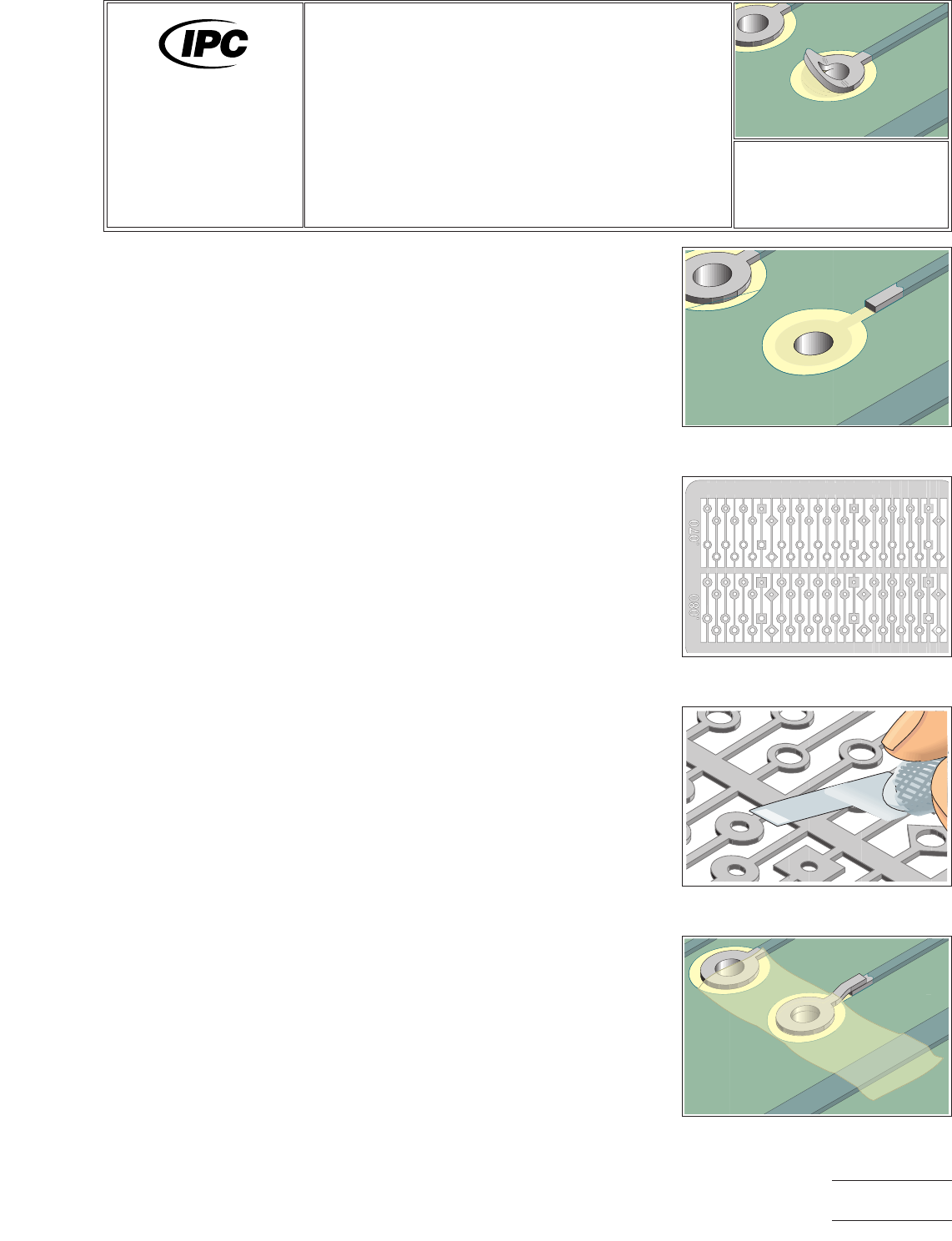
2. Remove the defective land and a short length of the connecting conductor if
any. (See Figure 1.)
Figure 1 Remove the defective land
and solder resist from the conductor.
Figure 2 Select a replacement land
that matches the missing land.
Figure 3 Cut out the replacement
land.
Figure 4 Place the new land in place
using tape.
7721A
Repair and
Modification of
Printed Boards and
Electronic Assemblies
Revision:
Date: 2/98
Land Repair,
Epoxy Method
Number: 4.5.1
Product Class: R, F
Skill Level: Advanced
Level of Conformance: Medium
Material in this manual was voluntarily established by Technical Committees of IPC. This material is advisory only and its use
or adaptation is entirely voluntary. IPC disclaims all liability of any kind as to the use, application, or adaptation of this material.
Users are also wholly responsible for protecting themselves against all claims or liabilities for patent infringement. Equipment
referenced is for the convenience of the user and does not imply endorsement by IPC.
Page1of4
Copyright Association Connecting Electronics Industries
Provided by IHS under license with IPC
Not for Resale
No reproduction or networking permitted without license from IHS
--``,``,-`-`,,`,,`,`,,`---
3. Use the knife and scrape off any epoxy residue, contamination or burned mate-
rial from the board surface.
CAUTION
Abrasion operations can generate electrostatic charges.
4. Scrape off any solder resist or coating from the connecting conductor. (See Fig-
ure 1.)
5. Clean the area.
6. Apply a small amount of liquid flux to the connection area on the board surface
and tin with solder. Clean the area. The length of the overlap solder connection
should be a minimum of 2 times the conductor width.
7. The area for the new pad on the board surface must be smooth and flat. If
internal fibers of the board are exposed or if there are deep scratches in the
surface they should be repaired. Refer to appropriate procedure.
8. Select a replacement land that most closely matches the land to be replaced.
(See Figure 2.)
9. Cut out and trim the new land. Cut the length to provide the maximum allow-
able conductor overlap for soldering. Minimum 2 times the conductor width.
(See Figure 3.)
NOTE
The new replacement land may be trimmed from copper sheet.
10. Mix the epoxy and apply a small amount to the surface where the new land will
be placed.
11. Place a piece of Polyimide tape over the top surface of the land. Place the new
land into position on the printed wiring board surface using the tape to aid in
alignment. (See Figure 4.)
12. Cure the epoxy per the manufacturer’s instructions.
13. After the epoxy has cured, remove the tape used for the alignment. Carefully
clean the area and inspect the new land for proper alignment.
NOTE
If the configuration permits, the overlap solder joint connection should be a
minimum of 3.00 mm from the related termination. This gap will minimize the
possibility of simultaneous reflow during soldering operations.
14. Remove tape and clean the area.
15. Mix the epoxy and coat the lap solder joint connections. Cure the epoxy per the
manufacturer’s recommended instructions.
NOTE
Additional epoxy can be applied around the perimeter of the new land to pro-
vide additional bond strength.
CAUTION
Some components may be sensitive to high temperature.
16. Carefully remove any excess epoxy inside the plated hole using a ball mill or drill
bit. Turn the ball mill or drill bit by hand to prevent damage to the wall of the
plated through hole.
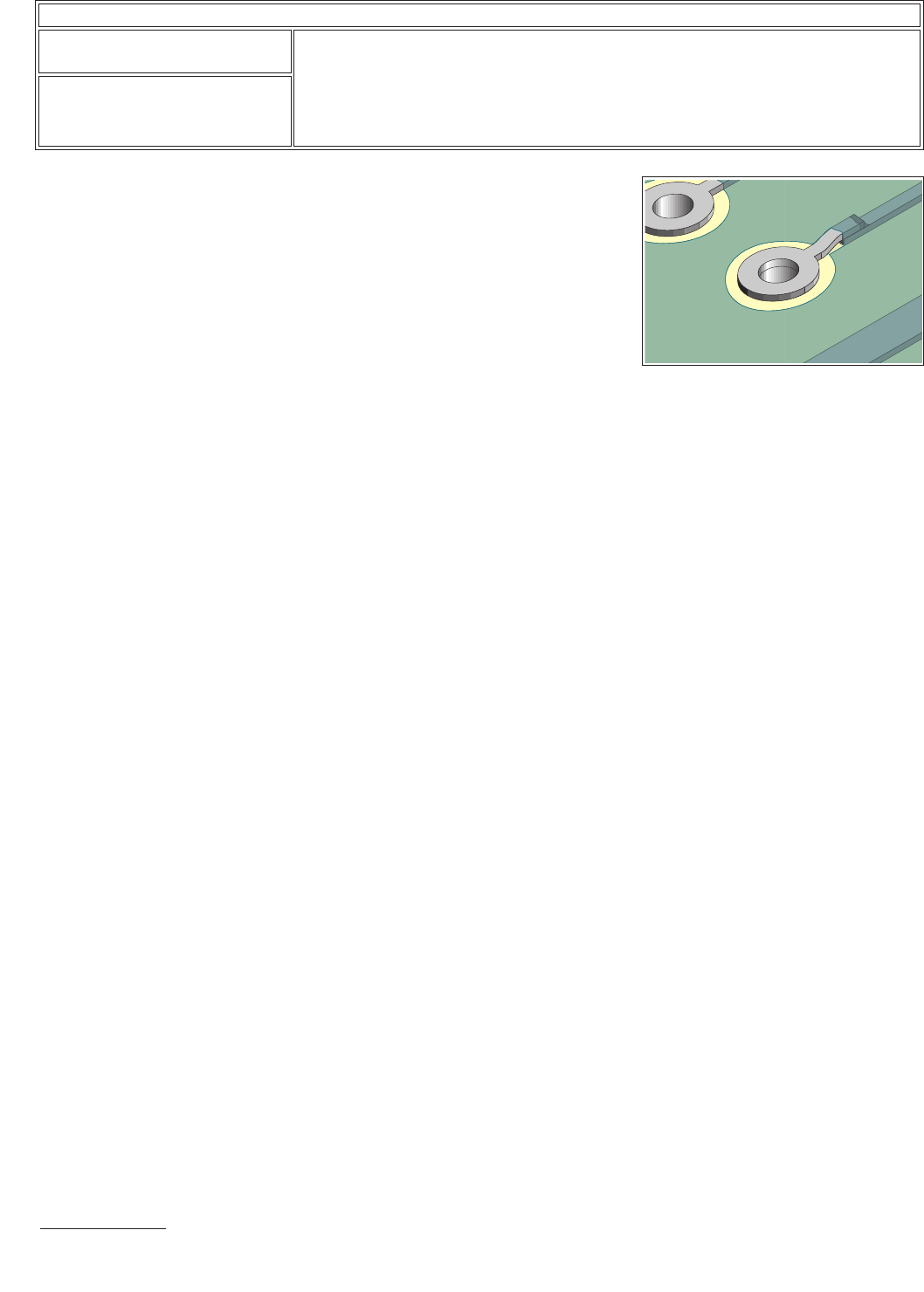
Figure 5 Completed repair.
IPC-7721A
Number: 4.5.1
Revision:
Date: 2/98
Subject: Land Repair, Epoxy Method
Page2of4
Copyright Association Connecting Electronics Industries
Provided by IHS under license with IPC
Not for Resale
No reproduction or networking permitted without license from IHS
--``,``,-`-`,,`,,`,`,,`---

17. Install the proper component and solder in place.
NOTE
This method is used to replace a damaged or missing lands, but the new land
will not have an intermetallic connection to the remaining plated hole. The sol-
der joint of the replaced component will restore the integrity of the electrical
connection or an eyelet or clinched buss wire may be used. See Plated Hole
Repair Procedures.
18. Apply surface coating to match prior coating as required.
EVALUATION
1. Visual examination
2. Measurement of new pad width and spacing.
3. Electrical continuity measurement.
IPC-7721A
Number: 4.5.1
Revision:
Date: 2/98
Subject: Land Repair, Epoxy Method
Page3of4
Copyright Association Connecting Electronics Industries
Provided by IHS under license with IPC
Not for Resale
No reproduction or networking permitted without license from IHS
--``,``,-`-`,,`,,`,`,,`---