IPC 7711A.pdf - 第29页
OUTLINE Electrostatic Discharge (ESD) is the rapid discharge of electri- cal energy that was created from static sources. When the electrical energy is allowed to come in contact with or even close to a sensitive compone…

generally more economical, CCTV systems offer greater
ease of use and less operator fatigue, particularly with very
fine pitch SMDs. See IPC-OI-645 for further information
on optical inspection equipment.
Component handling systems which can adequately estab-
lish and maintain X, Y, Z and THETA positioning are also
essential for successful alignment and placement during
fine pitch SMD installation.
1.9.7 Selecting Optimum Process for Manual Assembly/
Rework
Other than reasons such as purchase and life
cycle costs of equipment, operator training and learning
curves as well as other economic considerations, selecting
the optimum process for manual assembly/rework depends
on a variety of factors. These include:
• Type of component
– lead (termination) type
– body composition
• Size of component
• Type of substrate (FR-4, ceramic, etc.)
• Component mounting site
– thermal mass considerations
– adjacent components
– accessibility of component or joints
• Whether the component is being installed or removed
• Whether the component being removed must be salvaged
• Applicable workmanship specifications
• EOS/ESD control requirements
Every manual assembly/rework process and its attendant
equipment has advantages and precautions in each particu-
lar component installation or removal situation. For this
reason, the Procedures contained herein recommend par-
ticular processes for each individual component
installation/removal situation.
1.9.8 BGA/CSP/Flip Chip Time Temperature Profile
(TTP)
Because the terminations and connections of BGA,
CSP and Flip Chips are under the component, the operator
does not have the flexibility to modify the rework proce-
dure in process or visually inspect the end results. To
ensure acceptable results of the rework procedure, it is
critical to establish a time temperature profile for the
rework process. The following steps are needed to achieve
an acceptable TTP:
A preheat temperature for both the BGA and Printed Wir-
ing Assembly (PWA) (both ceramic and plastic* BGA’s
shall be preheated, as shall all PWA’s).
*
NOTE: If plastic body or tape bodied components are used,
see IPC J-STD-020 (Moisture/Reflow Sensitivity Classifica-
tion for Plastic Integrated Circuit Surface Mount Devices) for
information on moisture sensitivity classification tests, precon-
ditioning, and attachment.
Solder paste characteristics must be identified including
viscosity, thixotropy, rheology, deposition thickness and
drying time/temperature; or if using flux cored wire solder,
land prefill solder quantity and prefill coplanarity required.
Define a cleaning procedure which will meet the end item
cleanliness requirements of the customer.
Confirm the destructive physical examination and/or x-ray
analysis that the process defined will yield a BGA attach-
ment which meets any quality/reliability requirements
imposed.
Define, if used, an accelerated cooling system which does
not exceed thermal gradient limits of the most sensitive
component of the PWA.
CAUTION: THE TIME TEMPERATURE PROFILE IS DEPEN-
DENT, IN PART, ON AMBIENT RELATIVE HUMIDITY. RELA-
TIVE HUMIDITY VARIATIONS OF GREATER ± 15% FROM
THOSE PREVAILING WHEN THE TTP WAS ESTABLISHED
MAY REQUIRE MODIFICATION OF THE PROCEDURE
DEFINED DURING TTP.
1.9.9 Lead Free Solder
The rework of circuit boards
assembled using lead free solders are similar to common
alloys except as noted below. Proper training needs to be in
place to ensure quality and reliability of the assembly. Gen-
erally all that is needed is to understand those differences.
Those differences are:
• In most cases the newer alloys will require more time and
temperature and one must understand why
• The melting point of the solder alloys are likely to be
higher and thus may require a modified flux chemistry
• Wetting times are generally extended
• Solderability indicators such as wetting angles, joint
appearance etc., will generally be different
• Higher temperatures and longer dwell times may increase
oxidation
• Component lead frames as well as circuit board finishes
must be compatible with the solder alloy
• Using alternative means of attachment for rework/repair
(such as conductive epoxies) may be advantages due to
temperature and other considerations
• For both conductive and convective assembly rework/
repair, the use of inert atmosphere (such as nitrogen)
should be considered to facilitate the process
October 2003 IPC-7711A/7721A
9
Copyright Association Connecting Electronics Industries
Provided by IHS under license with IPC
Not for Resale
No reproduction or networking permitted without license from IHS
--``,``,-`-`,,`,,`,`,,`---
OUTLINE
Electrostatic Discharge (ESD) is the rapid discharge of electri-
cal energy that was created from static sources. When the
electrical energy is allowed to come in contact with or even
close to a sensitive component it can cause damage to the
component. Electrostatic-Discharge Sensitive (ESDS) compo-
nents are those components that are affected by these high
energy surges. The relative sensitivity of a component to ESD
is dependent upon its construction and materials. As compo-
nents become smaller and operate faster, the sensitivity
increases.
Electrical Overstress (EOS) is the internal result of a unwanted
application of electrical energy that results in damaged com-
ponents This damage can be from many different sources,
such as electrically powered process equipment or ESD
occurring during handling or processing.
ESDS components can fail to operate or change in value as a
result of improper handling or processing. These failures can
be immediate or latent. The result of immediate failure can be
additional testing and rework or scrap. However the conse-
quences of latent failure are the most serious. Even though
the product may have passed inspection and functional test,
it may fail after it has been delivered to the customer.
It’s important to build protection for ESDS components into
circuit designs and packaging. However, in the manufacturing
and assembly areas, we often work with unprotected elec-
tronic assemblies that are attached to the ESDS components.
This section will be dedicated to safe handling of these unpro-
tected electronic assemblies.
For that purpose, the following subjects are addressed:
2.1.1 Electrical Overstress (EOS) Damage Prevention
2.1.2 Electrostatic Discharge (ESD) Damage Prevention
2.1.3 Physical Handling
Information in this specification is intended to be general in
nature. Additional detailed information can be found in EIA-
625, Requirements for Handling Electrostatic-Discharge-
Sensitive (ESDS) Devices
2.1.1 Electrical Overstress (EOS) Damage Prevention
Electrical components can be damaged by unwanted electri-
cal energy from many different sources. This unwanted elec-
trical energy can be the result of ESD potentials or the result
of electrical spikes caused by the tools we work with, such as
soldering irons, soldering extractors, testing instruments or
other electrically operated process equipment. Some devices
are more sensitive than others. The degree of sensitivity is a
function of the design of the device. Generally speaking higher
speed and smaller devices are more susceptible than their
slower, larger predecessors. The purpose or family of the
device also plays an important part in component sensitivity.
This is because the design of the component can allow it to
react to smaller electrical sources or wider frequency ranges.
With todays products in mind, we can see that EOS is a more
serious problem than it was even a few years ago. It will be
even more critical in the future.
When considering the susceptibility of the product we must
keep in mind the susceptibility of the most sensitive compo-
nent in the assembly. Applied unwanted electrical energy can
be processed or conducted just as an applied signal would be
during circuit performance.
Before handling or processing sensitive components, tools
and equipment need to be carefully tested to ensure that they
do not generate damaging energy, including spike voltages.
Current research indicates that voltages and spikes less than
0.5 volt are acceptable. However, an increasing number of
extremely sensitive components require that soldering irons,
solder extractors, test instruments and other equipment must
never generate spikes greater than 0.3 volt.
As required by most ESD specifications including EIA-625,
periodic testing may be warranted to preclude damage as
equipment performance may degrade with use over time.
Maintenance programs are also necessary for process equip-
ment to ensure the continued ability to not cause EOS dam-
age.
EOS damage is certainly similar in nature to ESD damage,
since damage is the result of undesirable electrical energy.
2.1.2 Electrostatic Discharge (ESD) Damage Prevention
The best ESD damage prevention is a combination of prevent-
ing static charges and eliminating static charges if they do
occur. All ESD protection techniques and products address
one or both of the two issues.
Product Class: R, F, C, W
Skill Level: Intermediate
Level of Conformance: High
7711A/7721A
General Information and
Common Procedures
Revision: A
Date: 5/02
Handling Electronic
Assemblies
Number: 2.1
Material in this manual, IPC-7711 Rework of Electronic Assemblies, was voluntarily established by Technical Committees of
IPC. This material is advisory only and its use or adaptation is entirely voluntary. IPC disclaims all liability of any kind as to the
use, application, or adaptation of this material. Users are also wholly responsible for protecting themselves against all claims
or liabilities for patent infringement. Equipment referenced is for the convenience of the user and does not imply endorsement
by IPC.
Page1of4
Copyright Association Connecting Electronics Industries
Provided by IHS under license with IPC
Not for Resale
No reproduction or networking permitted without license from IHS
--``,``,-`-`,,`,,`,`,,`---
ESD damage is the result of electrical energy that was gener-
ated from static sources either being applied or in close prox-
imity to ESDS devices. Static sources are all around us. The
degree of static generated is relative to the characteristics of
the source. To generate energy relative motion is required.
This could be contacting, separation, or rubbing of the mate-
rial.
Most of the serious offenders are insulators since they con-
centrate energy where it was generated or applied rather than
allowing it to spread across the surface of the material. Com-
mon materials such as plastic bags or Styrofoam containers
are serious static generators and as such are not to be
allowed in processing areas especially static safe areas. Peel-
ing adhesive tape from a roll can generate 20,000 volts. Even
compressed air nozzles which move air over insulating sur-
faces generate charges.
Destructive static charges are often induced on nearby con-
ductors, such as human skin, and discharged into conduc-
tors. This can happen when a printed board assembly is
touched by a person having a static charge potential. The
electronic assembly can be damaged as the discharge
passes through the conductive pattern to a static sensitive
component. Static discharges may be too low to be felt by
humans (less than 3500 volts), and still damage ESDS
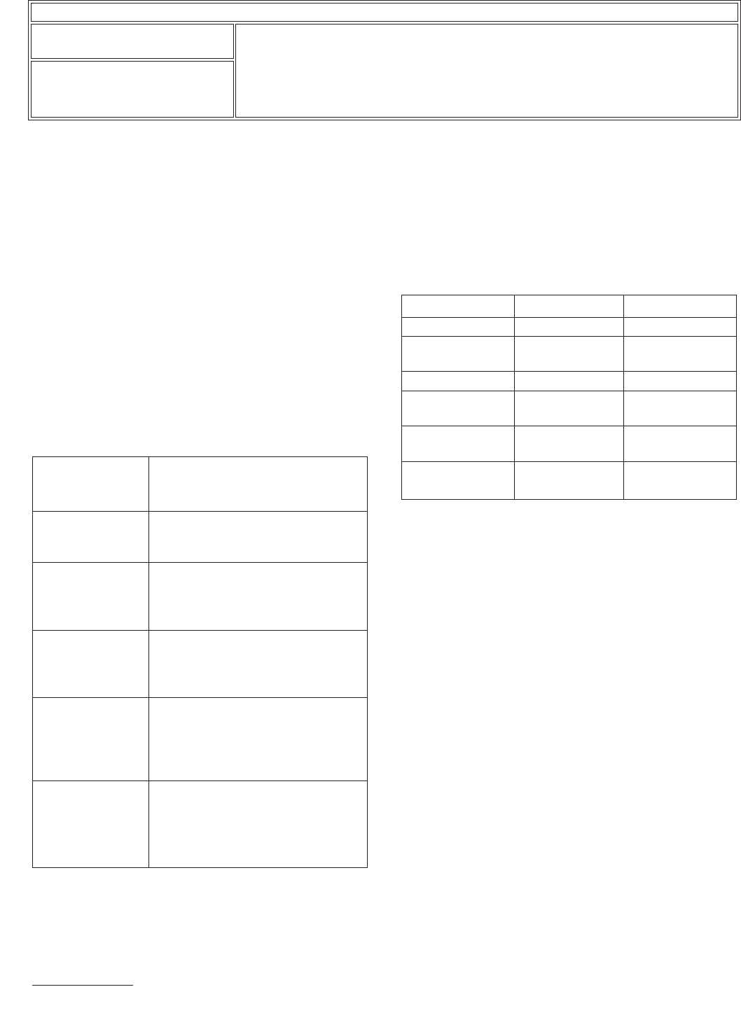
components. Typical static voltage generation is included in
Table 2.
2.1.3 Physical Handling
Care must be taken during acceptability inspections to ensure
product integrity at all times. Table 3 provides general guid-
ance.
Physical Damage
Improper handling can readily damage components and
assemblies (e.g., cracked, chipped or broken components
and connectors, bent or broken terminals, badly scratched
board surfaces and conductor lands). Physical damage of this
type can ruin the entire assembly or attached components.
Contamination
Contamination by handling with bare hands or fingers without
some form of protection causes soldering and coating prob-
lems; body salts and oils, and unauthorized hand creams are
typical contaminants. Body oils and acids reduce solderability,
promote corrosion and dendritic growth. They can also cause
poor adhesion of subsequent coatings or encapsulates.
Lotion formulated specifically for use in solder assembly areas
is available. Normal cleaning procedures will not always
remove such contaminants. The best solution is to prevent
contamination.
Table 1 Typical Static Charge Sources
Work surfaces Waxed, painted or varnished surfaces
Untreated vinyl and plastics
Glass
Floors Sealed concrete
Waxed or finished wood
Floor tile and carpeting
Clothes and
personnel
Non-ESD smocks
Synthetic materials
Non-ESD Shoes
Hair
Chairs Finished wood
Vinyl
Fiberglass
Non-conductive wheels
Packaging and
handling materials
Plastic bags, wraps, envelopes
Bubble wrap, foam
Styrofoam
Non-ESD totes, trays, boxes, parts
bins
Assembly tools and
materials
Pressure sprays
Compressed air
Synthetic brushes
Heat guns, blowers
Copiers, printers
Table 2 Typical Static Voltage Generation
Source 10-20% humidity 65-90% humidity
Walking on carpet 35,000 volts 1,500 volts
Walking on vinyl
flooring
12,000 volts 250 volts
Worker at a bench 6,000 volts 100 volts
Vinyl envelopes
(Work Instructions)
7,000 volts 600 volts
Plastic bag picked
up from the bench
20,000 volts 1,200 volts
Work chair with
foam pad
18,000 volts 1,500 volts
IPC-7711A/7721A
Number: 2.1
Revision: A
Date: 5/02
Subject: Handling Electronic Assemblies
Page2of4
Copyright Association Connecting Electronics Industries
Provided by IHS under license with IPC
Not for Resale
No reproduction or networking permitted without license from IHS
--``,``,-`-`,,`,,`,`,,`---