IPC 7711A.pdf - 第293页
EVALUATION 1. Visual examination 2. Measurement of new pad width and spacing. 3. Electrical continuity measurement. IPC-7721A Number: 4.7.1 Revision: Date: 2/98 Subject: Surface Mount Pad Repair , Epoxy Method P a g e3o …
5. Clean the area.
6. Apply a small amount of liquid flux to the connection area on the board surface
and tin with solder. Clean the area. The length of the overlap solder connection
should be a minimum of 2 times the conductor width.
7. The area for the new pad on the board surface must be smooth and flat. If
internal fibers of the board are exposed or if there are deep scratches in the
surface they should be repaired. Refer to appropriate procedure.
8. Select a commercially available surface mount pad that most closely matches
the surface mount pad to be replaced. If a special size or shape is needed they
can be custom fabricated.
9. Cut out and trim the new pad. Cut the length to provide the maximum allow-
able conductor overlap for soldering. Minimum 2 times the conductor width.
(See Figure 3.)
NOTE
The new replacement surface mount pad may be trimmed from copper sheet.
10. Mix the epoxy and apply a small amount to the surface where the new pad will
be placed.
11. Place a piece of Polyimide tape over the top surface of the new pad. Place the
new pad into position on the printed wiring board surface using the tape to help
in alignment. (See Figure 4.)
12. Cure the epoxy per the manufacturers instructions.
CAUTION
Some components may be sensitive to high temperature.
13. After the epoxy has cured remove the Polyimide tape used for alignment. Care-
fully clean the area and inspect the new pad for proper alignment.
14. If the new pad has a connecting conductor apply a small amount of liquid flux
to the lap solder joint connection area and solder the conductor from the new
pad to the conductor on the printed wiring board surface. Use minimal flux and
solder to ensure a reliable connection. Tape may be placed over the top of the
new pad to prevent excess solder overflow.
NOTE
If the configuration permits, the overlap solder joint connection should be a
minimum of 3.00 mm from the related termination. This gap will minimize the
possibility of simultaneous reflow during soldering operations.
15. Mix epoxy and coat the lap solder joint connections. Cure the epoxy per the
manufacturers recommended instructions.
NOTE
Additional epoxy can be applied around the perimeter of the new pad to pro-
vide additional bond strength.
16. Apply surface coating to match prior coating as required.
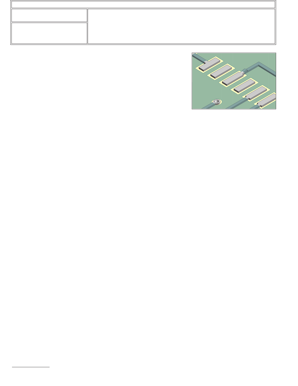
Figure 5 Completed repair.
IPC-7721A
Number: 4.7.1
Revision:
Date: 2/98
Subject: Surface Mount Pad Repair, Epoxy Method
Page2of4
Copyright Association Connecting Electronics Industries
Provided by IHS under license with IPC
Not for Resale
No reproduction or networking permitted without license from IHS
--``,``,-`-`,,`,,`,`,,`---

EVALUATION
1. Visual examination
2. Measurement of new pad width and spacing.
3. Electrical continuity measurement.
IPC-7721A
Number: 4.7.1
Revision:
Date: 2/98
Subject: Surface Mount Pad Repair, Epoxy Method
Page3of4
Copyright Association Connecting Electronics Industries
Provided by IHS under license with IPC
Not for Resale
No reproduction or networking permitted without license from IHS
--``,``,-`-`,,`,,`,`,,`---

NOTES
IPC-7721A
Number: 4.7.1
Revision:
Date: 2/98
Subject: Surface Mount Pad Repair, Epoxy Method
Page4of4
Copyright Association Connecting Electronics Industries
Provided by IHS under license with IPC
Not for Resale
No reproduction or networking permitted without license from IHS
--``,``,-`-`,,`,,`,`,,`---