IPC 7711A.pdf - 第296页
4. Scrape off any solder resist or coating from the connecting circuit. (See Figure 2.) 5. Clean the area. 6. Apply a small amount of liquid flux to the connection area on the board surface and tin with solder. Clean the…
OUTLINE
This method is used to replace damaged surface mount pads with new dry film,
adhesive backed pads. The new pads are bonded to the printed wiring board sur-
face using a specially designed bonding press or bonding iron.
CAUTION
It is essential that the board surface be smooth and flat. If the base material is dam-
aged see appropriate procedure.
NOTE
This method uses commercially available replacement surface mount pads. The new
pads are fabricated from copper foil. They are available in hundreds of sizes and
shapes and are generally supplied solder plated. If a special size or shape is needed
they can be custom fabricated.
REFERENCES
2.1 Handling Electronic Assemblies
2.2 Cleaning
2.5 Baking and Preheating
2.6 Epoxy Mixing and Handling
TOOLS & MATERIALS
Bonding Iron
Bonding System
Bonding Tips
Cleaner
Epoxy
Heat Lamp
Polyimide Tape
Knife
Liquid Flux
Microscope
Oven
Replacement Surface
Mount Pads
Scraper
Solder
Soldering Iron
Tweezers
Wipes
PROCEDURE
1. Clean the area.
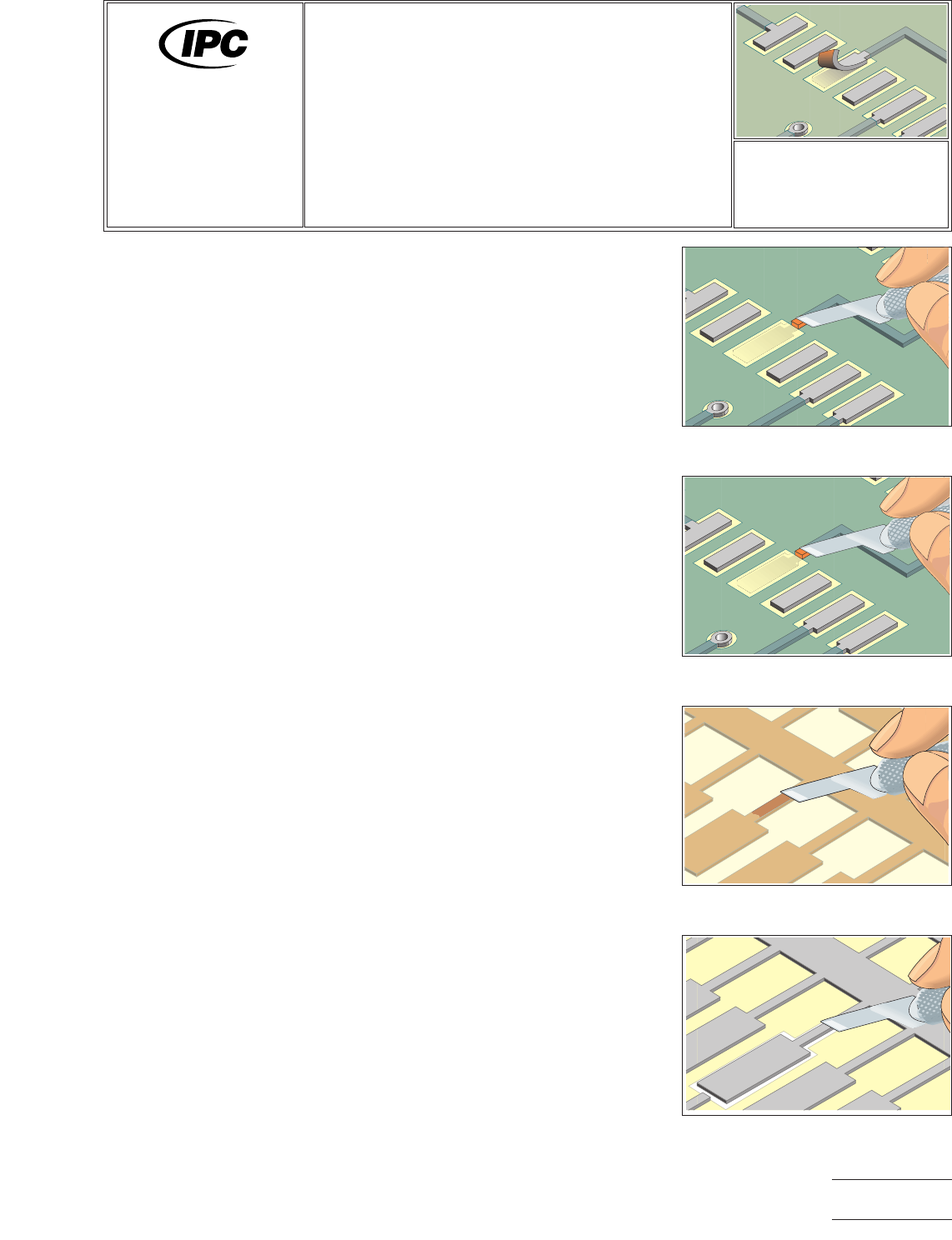
2. Remove the defective pad and a short length of the connecting circuit. (See
Figure 1.)
3. Use a knife and scrape off any epoxy residue, contamination or burned material
from the board surface.
CAUTION
Abrasion operations can generate electrostatic charges.
Figure 1 Remove the defective
surface mount pad and soldermask.
Figure 2 Scrape off solder resist.
Figure 3 Scrape off the adhesive
bonding film from solder joint area.
Figure 4 Cut out the new surface
mount pad.
7721A
Repair and
Modification of
Printed Boards and
Electronic Assemblies
Revision:
Date: 2/98
Surface Mount Pad
Repair, Film Adhesive
Method
Number: 4.7.2
Product Class: R, F, C
Skill Level: Advanced
Level of Conformance: High
Material in this manual was voluntarily established by Technical Committees of IPC. This material is advisory only and its use
or adaptation is entirely voluntary. IPC disclaims all liability of any kind as to the use, application, or adaptation of this material.
Users are also wholly responsible for protecting themselves against all claims or liabilities for patent infringement. Equipment
referenced is for the convenience of the user and does not imply endorsement by IPC.
Page1of4
Copyright Association Connecting Electronics Industries
Provided by IHS under license with IPC
Not for Resale
No reproduction or networking permitted without license from IHS
--``,``,-`-`,,`,,`,`,,`---
4. Scrape off any solder resist or coating from the connecting circuit. (See Figure
2.)
5. Clean the area.
6. Apply a small amount of liquid flux to the connection area on the board surface
and tin with solder. Clean the area. The length of the overlap solder connection
should be a minimum of 2 times the circuit width.
7. The area for the new pad on the board surface must be smooth and flat. If
internal fibers of the board are exposed or if there are deep scratches in the
surface, they should be repaired. Refer to appropriate procedure.
8. Select a commercially available surface mount pad that most closely matches
the surface mount pad to be replaced. If a special size or shape is needed they
can be custom fabricated.
NOTE
New surface mount pads are fabricated from copper foil. The foil is plated on
the top side with solder and an adhesive bonding film is applied to the bottom
side.
9. Before trimming out the new pad carefully scrape off the adhesive bonding film
from the solder joint connection area on the back of the new pad. (See Figure
3.)
CAUTION
Scrape off the epoxy backing only from the joint connection area. When han-
dling the replacement contact, avoid touching the epoxy backing with your fin-
gers or other materials that may contaminate the surface and reduce the bond
strength.
10. Cut out and trim the new pad. Cut out from the plated side. Cut the length to
provide the maximum allowable circuit overlap for soldering. Minimum 2 times
the circuit width. (See Figure 4.)
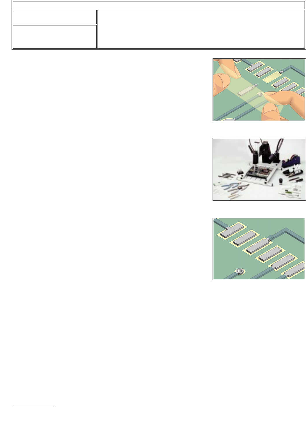
11. Place a piece of Polyimide tape over the top surface of the new pad. Place the
new pad into position on the printed wiring board surface using the tape to help
in alignment. Leave the tape in place during the bonding cycle. (See Figure 5.)
12. Select a commercially available bonding tip with a shape to match the shape of
the new pad. See bonding tip chart in the replacement parts section of the
manual provided with the repair system or repair kit.
NOTE
The tip used for bonding should be as small as possible but should completely
cover the entire surface of the new pad.
13. Position the printed wiring board so that it is flat and stable. Gently place the hot
bonding tip onto the tape covering the new pad. Apply pressure as recom-
mended in the manual of the repair system or repair kit. (See Figure 6.)
CAUTION
Excessive bonding pressure may cause measling in the printed wiring board
surface or may cause the new pad to slide out of position.
Figure 5 Place the new surface mount
pad in place using tape.
Figure 6 Bonding system.
Figure 7 Completed repair.
IPC-7721A
Number: 4.7.2
Revision:
Date: 2/98
Subject: Surface Mount Pad Repair, Film Adhesive Method
Page2of4
Copyright Association Connecting Electronics Industries
Provided by IHS under license with IPC
Not for Resale
No reproduction or networking permitted without license from IHS
--``,``,-`-`,,`,,`,`,,`---

14. After the timed bonding cycle lift the bonding iron and remove the tape used for
alignment. The pad is fully cured. Carefully clean the area and inspect the new
pad for proper alignment.
15. If the new pad has a connecting circuit apply a small amount of liquid flux to the
lap solder joint connection area and solder the circuit from the new pad to the
circuit on the printed wiring board surface. Use minimal flux and solder to
ensure a reliable connection. Tape may be placed over the top of the new pad
to prevent excess solder overflow.
NOTE
If the configuration permits, the overlap solder joint connection should be a
minimum of 3.00 mm from the related termination. This gap will minimize the
possibility of simultaneous reflow during soldering operations.
16. Mix epoxy and coat the lap solder joint connection. Cure the epoxy per the
manufacturers recommended instructions.
NOTE
Additional epoxy can be applied around the perimeter of the new pad to pro-
vide additional bond strength.
CAUTION
Some components may be sensitive to high temperature.
17. Apply surface coating to match prior coating as required.
EVALUATION
1. Visual examination
2. Measurement of new pad width and spacing.
3. Electrical continuity measurement.
IPC-7721A
Number: 4.7.2
Revision:
Date: 2/98
Subject: Surface Mount Pad Repair, Film Adhesive Method
Page3of4
Copyright Association Connecting Electronics Industries
Provided by IHS under license with IPC
Not for Resale
No reproduction or networking permitted without license from IHS
--``,``,-`-`,,`,,`,`,,`---