IPC 7711A.pdf - 第309页
12. Solder the eyelet to the exposed inner layer signal or plane by applying heat from a soldering iron to barrel of the eyelet. (See Figure 3.) 13. Completely remove any solder flux residue by spray rinsing with cleaner…
ID Inside Diameter
The eyelet inside diameter should be a 0.075 - 0.500 mm greater than the compo-
nent lead diameter.
LUF Length Under Flange
The length of the eyelet barrel under the flange should be 0.630 - 0.890 mm greater
than the thickness of the printed wiring board. This added length allows for proper
protrusion when setting the eyelet.
FD Flange Diameter
The eyelet flange diameter should be small enough to prevent interference with adja-
cent pads or conductors.
OD Outside Diameter
The clearance hole drilled through the printed wiring board should allow the eyelet to
be inserted without force but should not exceed 0.125 mm greater than the eyelet
outside diameter.
NOTE
Be sure to select an eyelet meeting the proper criteria. An eyelet with an oversize
flange may interfere with adjacent conductors. An eyelet that is too short will not
protrude through the printed wiring board for proper setting.
PROCEDURE
1. Clean the area.
2. Select an eyelet using the Eyelet Selection Criteria. Use a pin gauge and caliper
to measure the existing plated hole dimensions.
3. Pin the printed wiring board to the base of a precision drill press. (See Figure 1.)
4. Insert the appropriate ball mill, end mill or drill into the chuck of the drill press.
5. Mill or drill out the hole. The drilled hole should be approximately 0.030 mm
larger than the eyelet O.D. Inspect to ensure no metallic particles or burrs
remain.
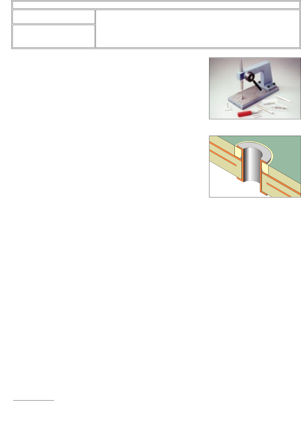
6. Select the side of the assembly that will have a counterbored hole milled into it.
This side preferably would have no surface connection.
7. Select an end mill approximately 0.050 - 0.075 mm larger than the eyelet diam-
eter. Insert into the precision drill press and mill down to and expose the inner
layer signal or plane. (See Figure 2.)
CAUTION
Great care must be taken to control the depth of the milled hole to prevent
damage to the inner layer signal or plane.
8. Clean the area.
9. Apply a small amount of flux to the exposed signal or plane and tin with solder.
10. Clean the area.
11. Insert the eyelet into the hole from the side opposite the milled hole, then apply
a small amount of flux into the milled hole.
Figure 5 Set the eyelet using an
eyelet press.
Figure 6 Eyelet barrel formed flat to
PC board surface.
IPC-7721A
Number: 5.3
Revision:
Date: 2/98
Subject: Plated Hole Repair, Inner Layer Connection
Page2of4
Copyright Association Connecting Electronics Industries
Provided by IHS under license with IPC
Not for Resale
No reproduction or networking permitted without license from IHS
--``,``,-`-`,,`,,`,`,,`---

12. Solder the eyelet to the exposed inner layer signal or plane by applying heat
from a soldering iron to barrel of the eyelet. (See Figure 3.)
13. Completely remove any solder flux residue by spray rinsing with cleaner.
14. Use a microscope and inspect the solder fillet from the eyelet to the inner con-
nection and perform electrical tests as required.
15. Mix epoxy as required.
16. Fill the milled hole with the epoxy up to, and level with, the surface of the board.
(See Figure 4.) The epoxy filler material should be free of voids and air bubbles.
17. Cure epoxy per the manufacturer’s recommendations
18. Select the proper setting tools and insert them into the eyelet press. (See Fig-
ure 5.)
19. Turn the printed wiring board over and rest the eyelet flange on the lower set-
ting tool.
20. Apply firm even pressure to form the eyelet barrel. (See Figure 6.)
21. Install the component lead and solder, if required.
22. Clean the area.
EVALUATION
1. Visual examination, dimensional requirement of pad diameter and inside diam-
eter.
2. Electrical continuity measurement.
IPC-7721A
Number: 5.3
Revision:
Date: 2/98
Subject: Plated Hole Repair, Inner Layer Connection
Page3of4
Copyright Association Connecting Electronics Industries
Provided by IHS under license with IPC
Not for Resale
No reproduction or networking permitted without license from IHS
--``,``,-`-`,,`,,`,`,,`---

NOTES
IPC-7721A
Number: 5.3
Revision:
Date: 2/98
Subject: Plated Hole Repair, Inner Layer Connection
Page4of4
Copyright Association Connecting Electronics Industries
Provided by IHS under license with IPC
Not for Resale
No reproduction or networking permitted without license from IHS
--``,``,-`-`,,`,,`,`,,`---