IPC 7711A.pdf - 第311页
OUTLINE This procedure covers the repair/modification of printed boards and electronic assemblies by the use of jumper wires to complete electrical continuity between two points. This procedure is meant to provide a foun…

NOTES
IPC-7721A
Number: 5.3
Revision:
Date: 2/98
Subject: Plated Hole Repair, Inner Layer Connection
Page4of4
Copyright Association Connecting Electronics Industries
Provided by IHS under license with IPC
Not for Resale
No reproduction or networking permitted without license from IHS
--``,``,-`-`,,`,,`,`,,`---
OUTLINE
This procedure covers the repair/modification of printed boards and electronic
assemblies by the use of jumper wires to complete electrical continuity between two
points. This procedure is meant to provide a foundation for adding jumper wires dur-
ing the repair/modification process. The techniques and guidelines are based on
general commercial and industry practices.
Jumper wires fall into three (3) categories
1. Those that are considered wires and are installed during assembly. The routing,
termination, and bonding of these jumper wires are documented by engineering
instructions or drawing notations.
2. Those that are added after assembly to effect a change or modification. The
routing, termination, and bonding of these jumper wires are documented by engi-
neering change notice instructions or drawing notations.
3. Those that are added to correct a defect.
This procedure has nine main sections.
1. References
2. Tools and Materials
3. General Rules
4. PC Board Preparation
5. Jumper Wire Selection
6. Jumper Wire Preparation
7. Jumper Wire Termination and Routing
8. Jumper Wire Bonding
9. Jumper Wire Termination Figures
REFERENCES
1.0 Foreword
2.1 Handling Electronic Assemblies
2.2 Cleaning
2.5 Baking and Preheating
TOOLS & MATERIALS
Adhesive, Hot Melt
Adhesive, Quick Set
Cleaner
Cleaning Wipes
Flush Cutter
Flux, Liquid
Smooth Pliers
Solder
Soldering Iron with Tips
Tape Dots
Wire
Wire, Adhesive Coated
Wire Stripper
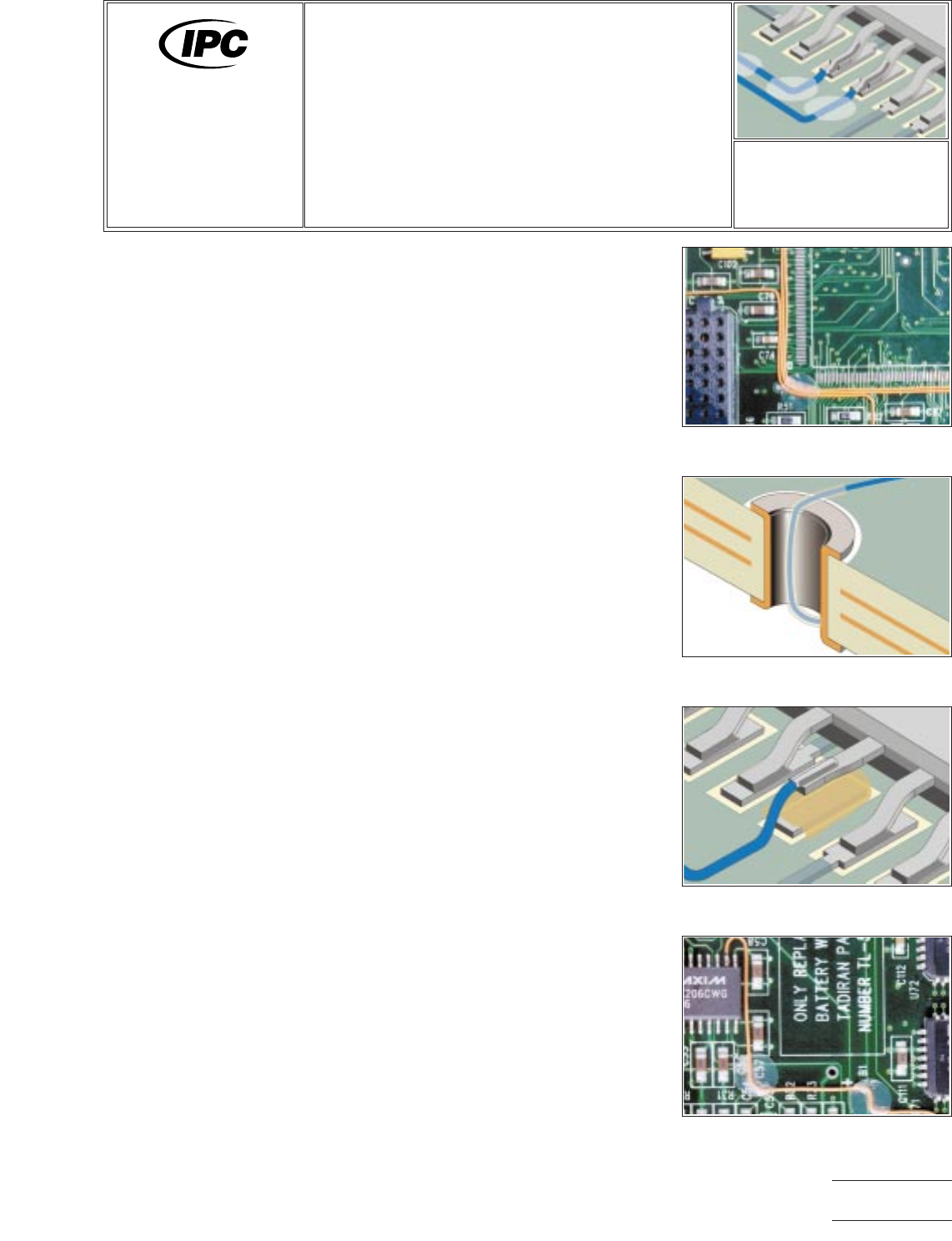
Figure 1 Route jumper wires.
Figure 2 Use sleeving through PTH.
Figure 3 Use insulated wire if
required.
Figure 4 Bond wires using tape dots
or strips.
7721A
Repair and
Modification of
Printed Boards and
Electronic Assemblies
Revision:
Date: 11/99
Jumper Wires
Number: 6.1
Product Class: R/F/W/C
Skill Level: Intermediate
Level of Conformance: N/A
Material in this manual was voluntarily established by Technical Committees of IPC. This material is advisory only and its use
or adaptation is entirely voluntary. IPC disclaims all liability of any kind as to the use, application, or adaptation of this material.
Users are also wholly responsible for protecting themselves against all claims or liabilities for patent infringement. Equipment
referenced is for the convenience of the user and does not imply endorsement by IPC.
Page1of10
Copyright Association Connecting Electronics Industries
Provided by IHS under license with IPC
Not for Resale
No reproduction or networking permitted without license from IHS
--``,``,-`-`,,`,,`,`,,`---
GENERAL RULES
1. Jumper wires should be placed on the component side of the assembly or
printed board unless otherwise specified.
2. Jumper wires shall be routed in an XY manner as directly as feasible, making as
few bends as possible. (See Figure 1.)
3. Jumper wires shall not be raised more than 3.2 mm [0.125 in] above the board
surface or not above components or leads in such a way that they will interfere
with PC board mounting.
4. Bare conductor jumper wires longer than 12.7 mm [0.50 in] shall not be used.
Bare conductor jumper wires shorter than 12.7 mm [0.50 in] shall not violate the
minimum electrical clearance.
NOTE
The 12.7 mm [0.50 in] dimension refers to the length between terminations.
5. Jumper wires may pass over lands provided sufficient slack is available so that
the wire can be moved away from the land for component replacement. Jumper
wires shall not pass over pads or vias used as test points.
6. Jumper wires shall not be routed under or over component leads or component
bodies. Contact with heat sinks must be avoided.
7. Jumper wires shall not pass through component foot prints unless the layout of
the assembly prohibits the routing in other areas.
8. Jumper wires shall have stress relief.
9. Jumper wires may be routed through plated through holes provided the wire is
insulated and insulation sleeving is placed in the hole. If a hole is needed, use
the following method. (See Figure 2.)
A. Drill a hole 0.25 mm [0.010 in] larger than the insulation diameter.
B. Inspect the hole for burs or exposed internal circuits.
C. Document the added hole on a control drawing.
NOTE
Be careful that the drilled hole does not interfere with surface and internal con-
ductors.
10. Jumper wires soldered into plated through holes must be discernible on the
opposite side.
11. Jumper wires soldered to lifted or clipped component leads may require insula-
tion to prevent shorting. (See Figure 3.)
12. Jumper wires may be terminated by a variety of methods. See illustrations.
PC BOARD PREPARATION
1. Clean the area.
NOTE
When wires are in place cleaning will often be more difficult.
2. Remove coating material or oxidization as necessary from the component leads,
pads, or conductors where wire terminations will be soldered. Clean the area.
Figure 5 Bond wires using adhesive.
Figure 6 Adhesive coated wires are
heat bonded.
IPC-7721A
Number: 6.1
Revision:
Date: 11/99
Subject: Jumper Wires
Page2of10
Copyright Association Connecting Electronics Industries
Provided by IHS under license with IPC
Not for Resale
No reproduction or networking permitted without license from IHS
--``,``,-`-`,,`,,`,`,,`---