IPC 7711A.pdf - 第326页
NOTES IPC-7721A Number: 6.2.2 Revision: Date: 10/03 Subject: Jumper Wires, BGA Components, Through Board Method P a g e4o f4 Copyright Association Connecting Electronics Industries Provided by IHS under license with IPC …
EVALUATION
1. Visual examination for alignment and overlap of foil jumper.
2. Visual examination of epoxy coating for texture and color match.
3. Electrical tests as applicable.
IPC-7721A
Number: 6.2.2
Revision:
Date: 10/03
Subject: Jumper Wires, BGA Components, Through Board Method
Page3of4
Copyright Association Connecting Electronics Industries
Provided by IHS under license with IPC
Not for Resale
No reproduction or networking permitted without license from IHS
--``,``,-`-`,,`,,`,`,,`---
NOTES
IPC-7721A
Number: 6.2.2
Revision:
Date: 10/03
Subject: Jumper Wires, BGA Components, Through Board Method
Page4of4
Copyright Association Connecting Electronics Industries
Provided by IHS under license with IPC
Not for Resale
No reproduction or networking permitted without license from IHS
--``,``,-`-`,,`,,`,`,,`---
OUTLINE
This procedure covers the general guidelines for modifications that involve adding
components.
REFERENCES
1.0 Index
2.1 Handling Electronic Assemblies
2.2 Cleaning
2.5 Baking and Preheating
TOOLS & MATERIALS
Cleaner
Cleaning Wipes
Flux
Microscope System
Soldering Iron with Tips
Solder
GENERAL RULES
1. Added components may need to be secured with adhesive, or by other means,
if the component leads or component body would be subjected to mechanical
stress.
2. Leads of added components should not be inserted into plated holes occupied
by another component lead.
3. Added components placed on the circuit board surface should be placed on the
component side of the assembly or circuit board unless otherwise specified.
4. Added components shall not be raised above the board surface beyond allow-
able dimensions.
5. Added components shall not cover over pads or vias used as test points.
6. Added components shall not cover other component foot prints unless the lay-
out of the assembly prohibits mounting in other areas.
7. Added component leads may require insulation to avoid contact with compo-
nent body or other conductors.
8. Removal of existing solder from a connection point may be necessary to avoid
bridging, or excess solder, in the final connection.
9. Consider design limitations and product use environments when stacking com-
ponents.
10. Do not exceed minimum component lead bend radius.
11. When possible, component identification marking shall be legible.
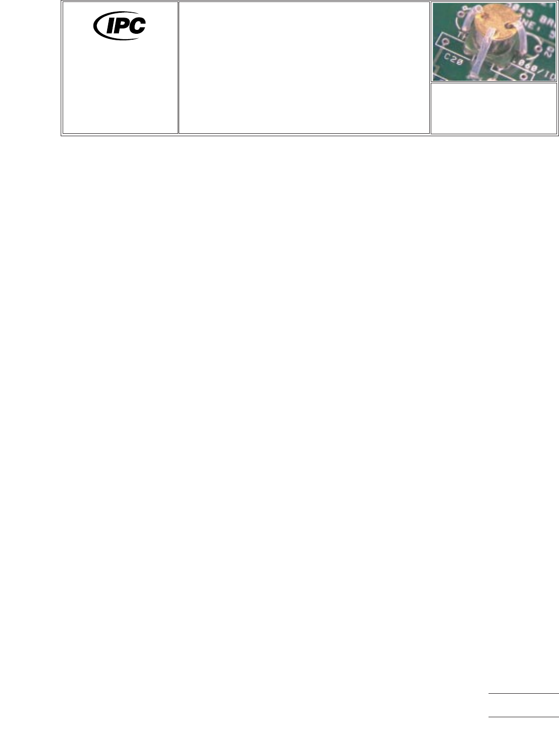
7721A
Repair and
Modification of
Printed Boards and
Electronic Assemblies
Revision:
Date: 03/01
Component Modifications
and Additions
Number: 6.3
Product Class: R,F,W,C
Skill Level: Advanced
Level of Conformance: N/A
Material in this manual was voluntarily established by Technical Committees of IPC. This material is advisory only and its use
or adaptation is entirely voluntary. IPC disclaims all liability of any kind as to the use, application, or adaptation of this material.
Users are also wholly responsible for protecting themselves against all claims or liabilities for patent infringement. Equipment
referenced is for the convenience of the user and does not imply endorsement by IPC.
Page1of4
Copyright Association Connecting Electronics Industries
Provided by IHS under license with IPC
Not for Resale
No reproduction or networking permitted without license from IHS
--``,``,-`-`,,`,,`,`,,`---