IPC 7711A.pdf - 第48页
EVALUATION 1. Visual examination or UV light may be used to verify complete removal of coating. NOTES IPC-771 1A/7721A Number: 2.3.6 Revision: Date: 2/98 Subject: Coating Removal, Macro Blasting Method P a g e2o f2 Copyr…
OUTLINE
This coating removal method uses a micro abrasive blasting system and a very fine
soft abrasive powder. The powder is propelled through a small nozzle toward the
area where the coating needs to be removed.
To determine the appropriate coating removal procedure the coating must first be
identified. Refer to procedure number 2.3.1.
CAUTION
Micro blasting will generate substantial static charges. The work area should be
flooded with ionized air and the printed wiring board assembly should be grounded
whenever possible.
REFERENCES
2.1 Handling Electronic Assemblies
2.2 Cleaning
2.3.1 Coating Removal, Identification of Conformal Coatings
2.4.1 Coating Replacement, Solder Resist
2.4.2 Coating Replacement, Conformal Coatings/Encapsulants
TOOLS AND MATERIALS
Abrasive Powder
Polyimide Tape
Micro Blasting System
Removable Mask
Stencils
PROCEDURE
1. Clean the area.
2. Select the appropriate abrasive blasting powder and nozzle size. Set the air pres-
sure at the desired setting per equipment manufacturer’s instructions.
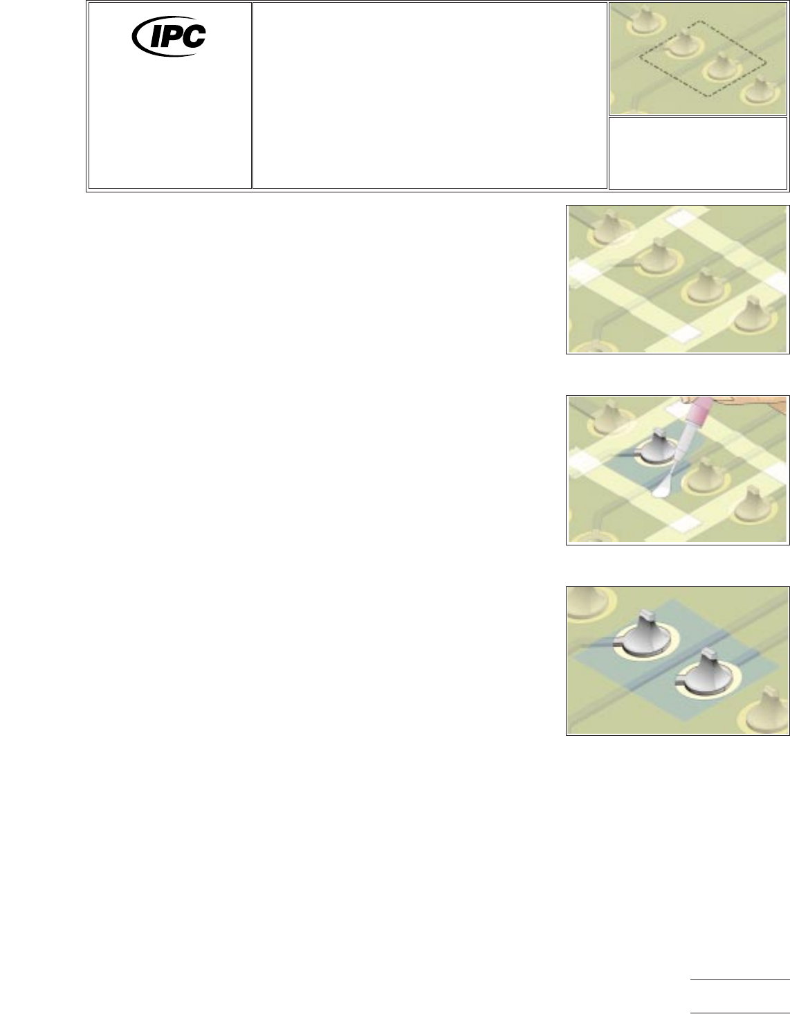
3. Apply polyimide tape or other masking material to protect the printed wiring board
surface as needed. (See Figure 1.) Masking materials can consist of tapes, cur-
able liquid masks or reusable stencils.
4. If the printed wiring board has static sensitive components, insert the entire
printed wiring board into a shielded bag. Only the area needing rework should be
exposed. Ground the printed wiring board to dissipate static charges if needed.
5. Insert the printed wiring board into the blasting chamber and blast away the
damaged or unwanted coating or solder resist. Slowly move the nozzle along the
area where the coating is to be removed. (See Figure 2.)
6. Blow off the blasting dust and clean the area.
Figure 1 Apply tape to outline area for
coating removal.
Figure 2 Remove coating using micro
blasting system.
Figure 3 Removal complete.
7711A/7721A
General
Information and
Common Procedures
Revision:
Date: 2/98
Coating Removal,
Micro Blasting
Method
Number: 2.3.6
Product Class: R, F, W, C
Skill Level: Advanced
Level of Conformance: High
Material in this manual was voluntarily established by Technical Committees of IPC. This material is advisory only and its use
or adaptation is entirely voluntary. IPC disclaims all liability of any kind as to the use, application, or adaptation of this material.
Users are also wholly responsible for protecting themselves against all claims or liabilities for patent infringement. Equipment
referenced is for the convenience of the user and does not imply endorsement by IPC.
Page1of2
Copyright Association Connecting Electronics Industries
Provided by IHS under license with IPC
Not for Resale
No reproduction or networking permitted without license from IHS
--``,``,-`-`,,`,,`,`,,`---

EVALUATION
1. Visual examination or UV light may be used to verify complete removal of coating.
NOTES
IPC-7711A/7721A
Number: 2.3.6
Revision:
Date: 2/98
Subject: Coating Removal, Macro Blasting Method
Page2of2
Copyright Association Connecting Electronics Industries
Provided by IHS under license with IPC
Not for Resale
No reproduction or networking permitted without license from IHS
--``,``,-`-`,,`,,`,`,,`---
OUTLINE
This method is used to replace solder resist or coatings on printed wiring boards.
Most replacement coatings can be applied by dipping, brushing or spraying.
REFERENCES
2.1 Handling Electronic Assemblies
2.2 Cleaning
2.5 Baking and Preheating
2.6 Epoxy Mixing and Handling
TOOLS & MATERIALS
Cleaner
Cleaning Wipes
Color Agent, Various Colors
Brush
Epoxy or Replacement Coating
Foam Swab
Heat Lamp
Microscope
Oven
PROCEDURE
1. Clean the area.
CAUTION
Surfaces to be coated must be thoroughly cleaned prior to coating to ensure
adequate adhesion, minimized corrosion, and optimized electrical properties.
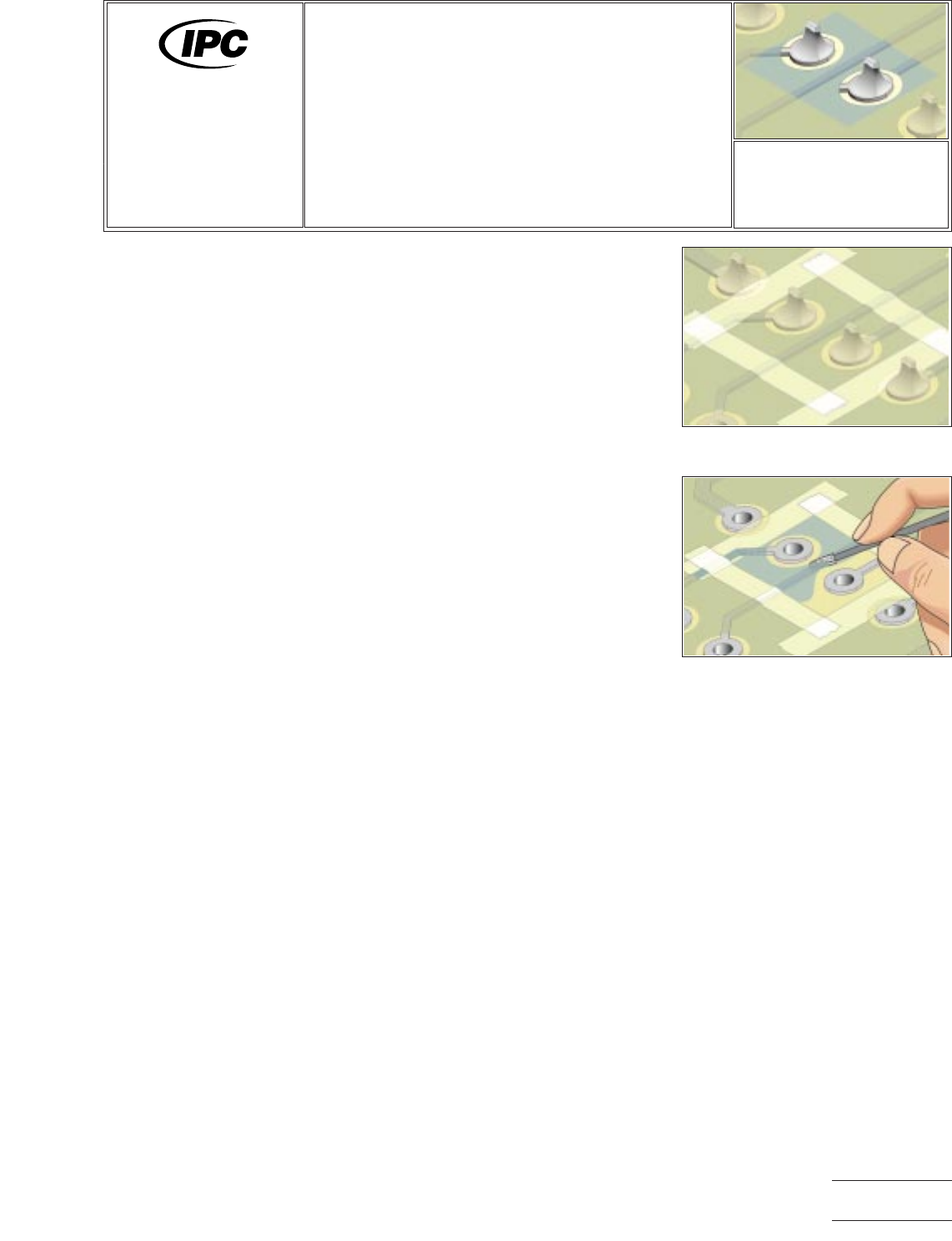
2. If needed, apply Polyimide tape to outline the area where the solder resist will be
applied. (See Figure 1.)
3. Mix the epoxy or replacement coating. If desired, add color agent to the mixed
epoxy to match the printed wiring board color.
4. Apply the replacement coating to the board surface as required. A brush or foam
swab may be used to apply and spread the epoxy or replacement coating. (See
Figure 2.)
5. Cure the replacement coating per the manufacturer’s instructions.
CAUTION
Some components may be sensitive to high temperature.
EVALUATION
1. Visual examination for texture, color match, adhesion and coverage.
2. Electrical tests to conductors around the repaired area as applicable.
Figure 1 Apply polyimide tape if
needed.
Figure 2 Apply replacement coating
with a foam swab to create a texture.
7711A/7721A
General
Information and
Common Procedures
Revision:
Date: 2/98
Coating Replacement,
Solder Resist
Number: 2.4.1
Product Class: R, F, W, C
Skill Level: Intermediate
Level of Conformance: High
Material in this manual was voluntarily established by Technical Committees of IPC. This material is advisory only and its use
or adaptation is entirely voluntary. IPC disclaims all liability of any kind as to the use, application, or adaptation of this material.
Users are also wholly responsible for protecting themselves against all claims or liabilities for patent infringement. Equipment
referenced is for the convenience of the user and does not imply endorsement by IPC.
Page1of2
Copyright Association Connecting Electronics Industries
Provided by IHS under license with IPC
Not for Resale
No reproduction or networking permitted without license from IHS
--``,``,-`-`,,`,,`,`,,`---