SMU_dat-sw-en.pdf - 第21页
Version 08.00, Januar y 2012 Rohde & Schwarz R&S ® SMU200A Vector Signal Generator 21 Differential I/Q output (R&S ® SMU-B16 option) One R&S ® SMU-B16 option can be installed; the I/Q output signals are a…
Version 08.00, January 2012
20 Rohde & Schwarz
R&S
®
SMU200A Vector Signal Generator
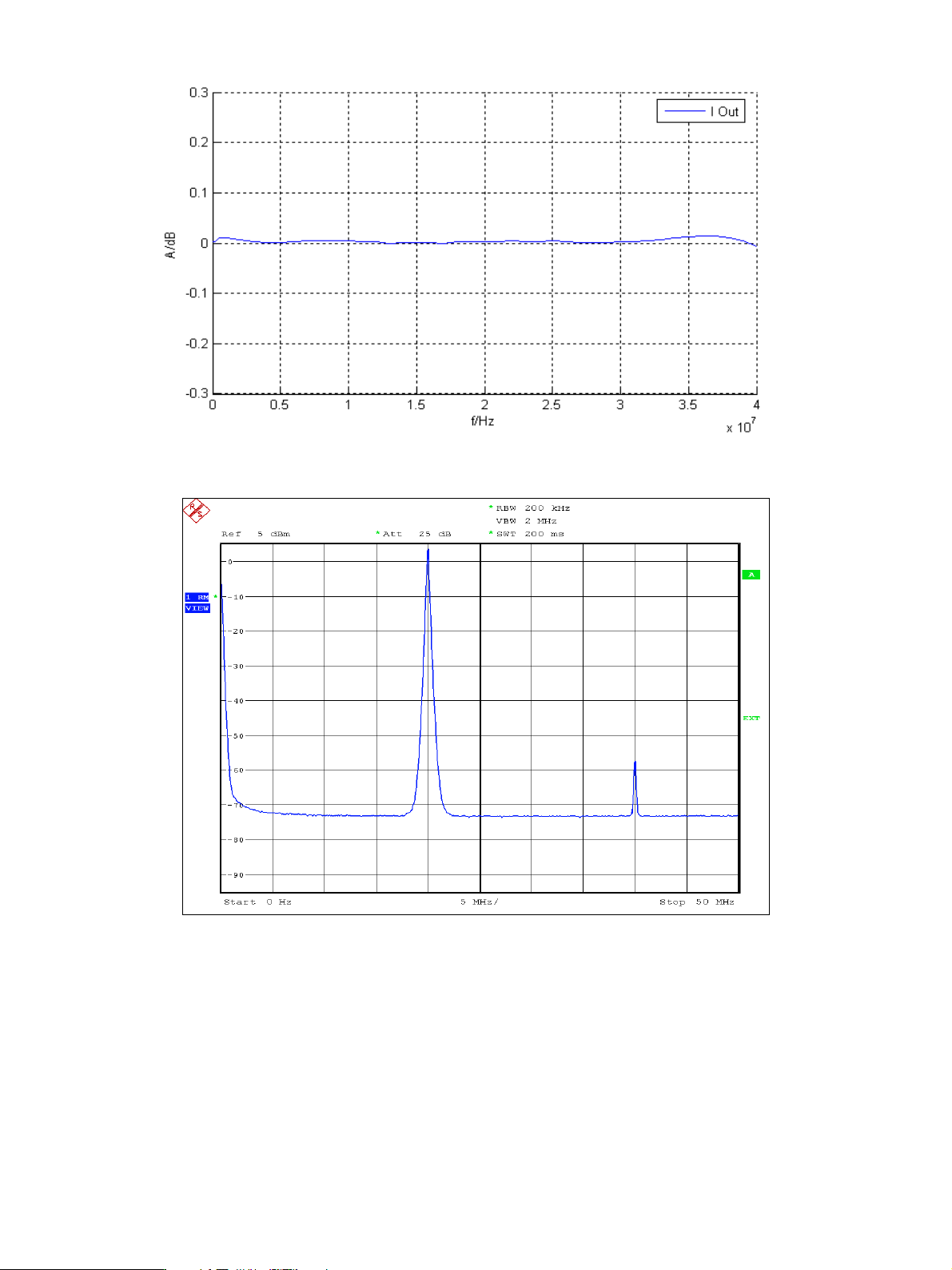
Measured frequency response of I/Q outputs.
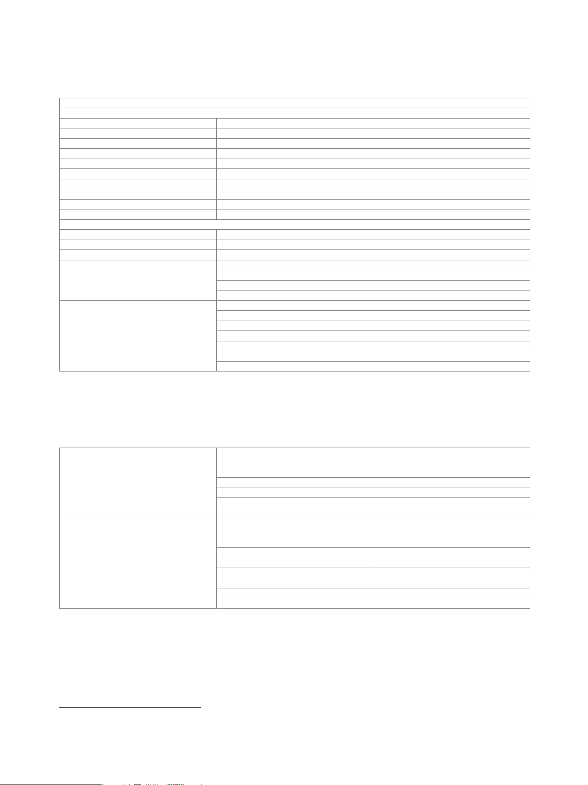
Measured SFDR of I/Q outputs.
Version 08.00, January 2012
Rohde & Schwarz R&S
®
SMU200A Vector Signal Generator 21
Differential I/Q output (R&S
®
SMU-B16 option)
One R&S
®
SMU-B16 option can be installed; the I/Q output signals are available either for path A or B.
This option is not compatible with rear-panel outputs (R&S
®
SMU-B81 and R&S
®
SMU-B82 options).
Additional specifications for I/Q outputs with R&S
®
SMU-B16 option
Output impedance
Single-ended 50
Differential 100
Output voltage output voltage depends on set modulation signal
Single-ended EMF 0.02 V to 2 V (V
p
)
Resolution 1 mV
Differential EMF 0.04 V to 4 V (V
pp
)
Resolution 2 mV
Bias voltage (single-ended and differential) EMF –3.6 V to +3.6 V
Resolution 2 mV
Uncertainty 1 % + 4 mV
Offset voltage
Differential EMF –300 mV to +300 mV
Resolution 0.2 mV
Uncertainty 1 % + 0.1 % × bias voltage + 1 mV
at R
L
= 50 , output voltage > 0.5 V (V
p
)
magnitude
up to 10 MHz < 0.2 dB, 0.05 dB (typ.)
Differential signal balance
up to 40 MHz 0.2 dB (typ.)
at R
L
= 50 , output voltage > 0.5 V
(V
p
)
magnitude
up to 10 MHz 0.02 dB (typ.)
up to 40 MHz 0.03 dB (typ.)
nonlinear phase
up to 10 MHz 0.1° (typ.)
Frequency response
5
up to 30 MHz 0.2° (typ.)
Digital baseband output (R&S
®
SMU-B18 option)
The R&S
®
SMU-B18 option makes digital I/Q signals available on the rear panel of the instrument. The digital I/Q output can be used
for the lossless connection of the R&S
®
SMU200A to the digital I/Q input of other Rohde & Schwarz instruments (e.g. R&S
®
AMU200A
baseband signal generator and fading simulator). One R&S
®
SMU-B18 can be installed.
standard
in line with Rohde & Schwarz TVR290,
I/Q data and control signals, data and
interface clock
level LVDS
connector 26-pin MDR
Interface
data rate 30 MHz to 100 MHz with 1 MHz resolution,
81.6 MHz
With source ‘user-defined’, the sample rate must be entered via the parameter ‘sample
rate’, no I/Q data clock being necessary. With source ‘digital I/Q out’ or ‘digital I/Q in’,
the sample rate will be estimated on the basis of the applied I/Q data clock.
source user-defined, digital I/Q out, digital I/Q in
sample rate 400 Hz to 100 MHz
max. sample rate limited by actual
interface data rate
resolution (user-defined) 0.001 Hz
I/Q sample rate
frequency uncertainty (user-defined) < 5 × 10
−
14
5
Optimize internal I/Q impairments for RF output switched off.
Version 08.00, January 2012
22 Rohde & Schwarz
R&S
®
SMU200A Vector Signal Generator
resolution 18 bit
logic format two’s complement
physical signal level
setting range 0 to –60 dBFS
resolution 0.01 dBFS
bandwidth
sample rate = 100 MHz
(no interpolation, user-defined)
40 MHz
I/Q data
sample rate < 100 MHz (interpolation) 0.31 × sample rate
markers 4 Control signals
data valid valid samples marked in data stream
Baseband input (analog/digital) (R&S
®
SMU-B17 option)
At least one R&S
®
SMU-B13 baseband main module and at least one R&S
®
SMU-B9/-B10/-B11 I/Q baseband generator must be
installed. The R&S
®
SMU-B17 option makes it possible to feed external analog or digital signals to the baseband section of the
R&S
®
SMU200A. The frequency of the signals can be shifted, and the signals can be added to the internally generated signal with
settable level ratio. If the R&S
®
SMU200A is equipped with a fading simulator, the input signals can also be faded.
Mode see also simultaneous modulation analog input,
digital input
peak level
setting range –10 dB to 0 dB referenced to full scale
resolution 0.01 dB
crest factor
setting range 0 dB to 30 dB
resolution 0.01 dB
Input level
The adjust level function automatically determines the peak level and crest factor of the
input signal.
The frequency offset can be used to shift the center frequency of the input signal in the
baseband. The restrictions caused by the modulation bandwidth apply.
setting range −40 MHz to +40 MHz
resolution 0.01 Hz
Frequency offset
frequency accuracy < 5 × 10
− 10 × frequency offset +
reference frequency error
I/Q swap I and Q signals swapped on/off
Analog I/Q inputs
All specifications apply to a peak level of 0 dB.
input impedance 50
VSWR up to 30 MHz < 1.1, 1.03 (typ.)
I/Q inputs
input voltage for full-scale input
q
22
i
+= 0.5 V
VV
carrier leakage I, Q
setting range −10 % to +10 %
resolution 0.01 %
I ≠ Q (imbalance)
setting range −3 dB to +3 dB
resolution 0.001 dB
I/Q skew
setting range –1 ns to +1 ns
I/Q impairment
resolution 1 ps
sample rate 100 MHz A/D converter
resolution 14 bit
with amplitude and group delay correction
bandwidth, roll-off to –0.1 dB 30 MHz
Aliasing filter
stopband rejection, f 70 MHz 80 dB (typ.)
I/Q wideband: on, optimize internal I/Q impairments for RF output: on
up to 10 MHz 0.2 dB (typ.)
RF frequency response for entire
instrument in modulation bandwidth
up to 30 MHz 0.4 dB (typ.)