HF Circuit .pdf - 第234页
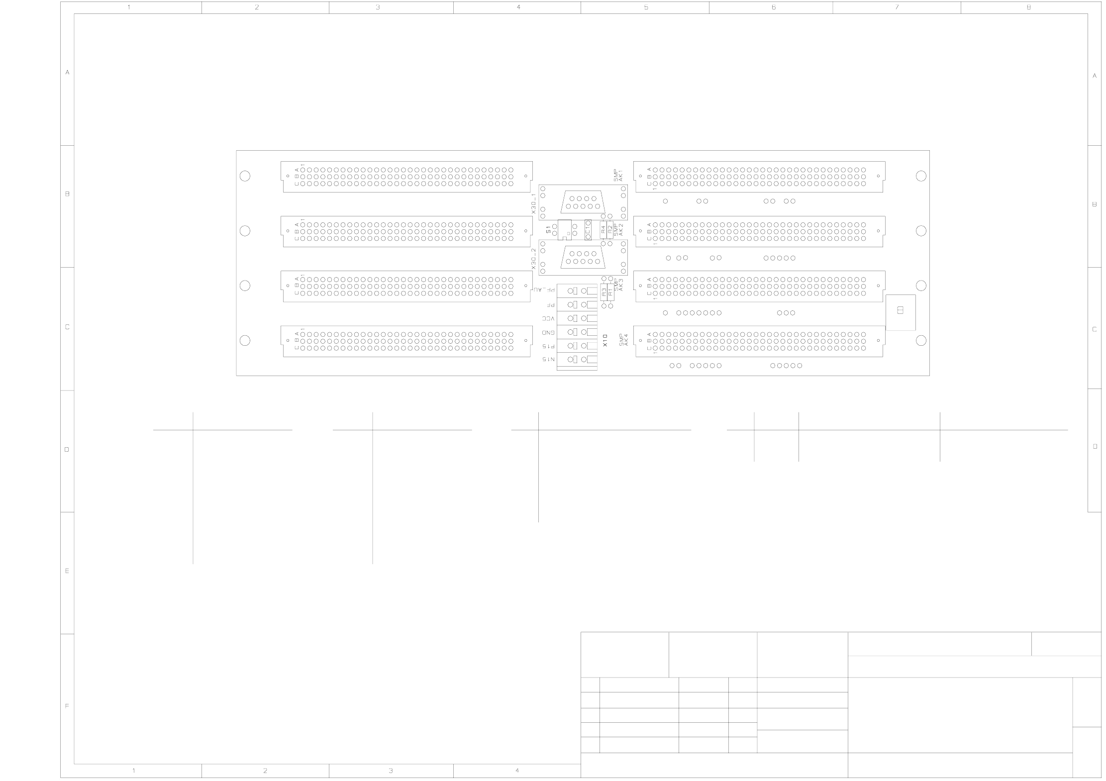
5 - 25 0035348 6-010 401ND3 Anti- crash backp lane / b allast circuit (Sh . 1 of 2 ) 0035348 6-010 401ND3 Backplane, anticrash / balla st cir cuit Component layout, co mponent s ide 1 : 1 KD KD G32918 - N0037 - U021 - * …
5 - 24
00353485-030101ND3 Backplane, axis, solder side (Sh. 2 of 2)
Comunicado como segredo empresarial. Reservados todos os direitos.
Confiado como secrete industrial. Nos reservamos todos los derechos.
Confie a titre de secret d'entreprise. Tous droits reserves.
Proprietary data, company confidential. All rights reserved.
nicht ausdrücklich zugestanden. Zuwiderhandlungen ver-
Weitergabe sowie Vervielfältigung dieser Unterlage,Ver-
wertung und Mitteilung ihres Inhalts nicht gestattet, soweit
besondere für den Fall der Patenterteilung oder GM-Eintragung
pflichten zu Schadenersatz. Alle Rechte vorbehalten, ins
B = Identification label
11 x 13
Component layout, solder side
Stat.
05
Format
Modified Date
23.03.05
SIEMENS EDM
Name SEDM E MCH
Name
Date
KD
Dorfner
02.08.01
00353485-030101ND3
Printed circuit board
SIPLACE HF series
Backplane, axis
Scale
1:1
Sheet
2 -
A3
ON
ON2
1
S1 HF/3 placement area 2HF/3 placement area 1
OFF
OFFON
OFF
HFX10
1
2
-15V
+15V
VCC
GND
4
3
Power failure
PowerFailureAxis
5
6GND
CAN_INT
Power failure
GND
CAN_L
1-Wire
3
6
5
4
2
1
X30_2
9
8
7
n.u.
RESET
CAN_H
CAN bus
Power failure
9n.u.
GND3
RESET
CAN_INT
GND
CAN_H
6
7
8
4
5
CAN bus
1-Wire
CAN_L
1
2
X30_1
5 - 25
00353486-010401ND3 Anti-crash backplane / ballast circuit (Sh. 1 of 2)
00353486-010401ND3
Backplane, anticrash / ballast circuit
Component layout, component side
1 : 1
KD
KD
G32918 - N0037 - U021 - * - 17
KD
Name
KD
ModifiedStat.
01.
02.
03.
04.
30.08.01
27.04.01
18.02.02
Date
06.11.02 27.04.01
2-layer PCB
SIEMENS AG
Name
MCH2
I&S IS
Dorfner
Date
PC board
Scale
989
1 +
Sheet
C = revision label
B = inspection label
A = identification label
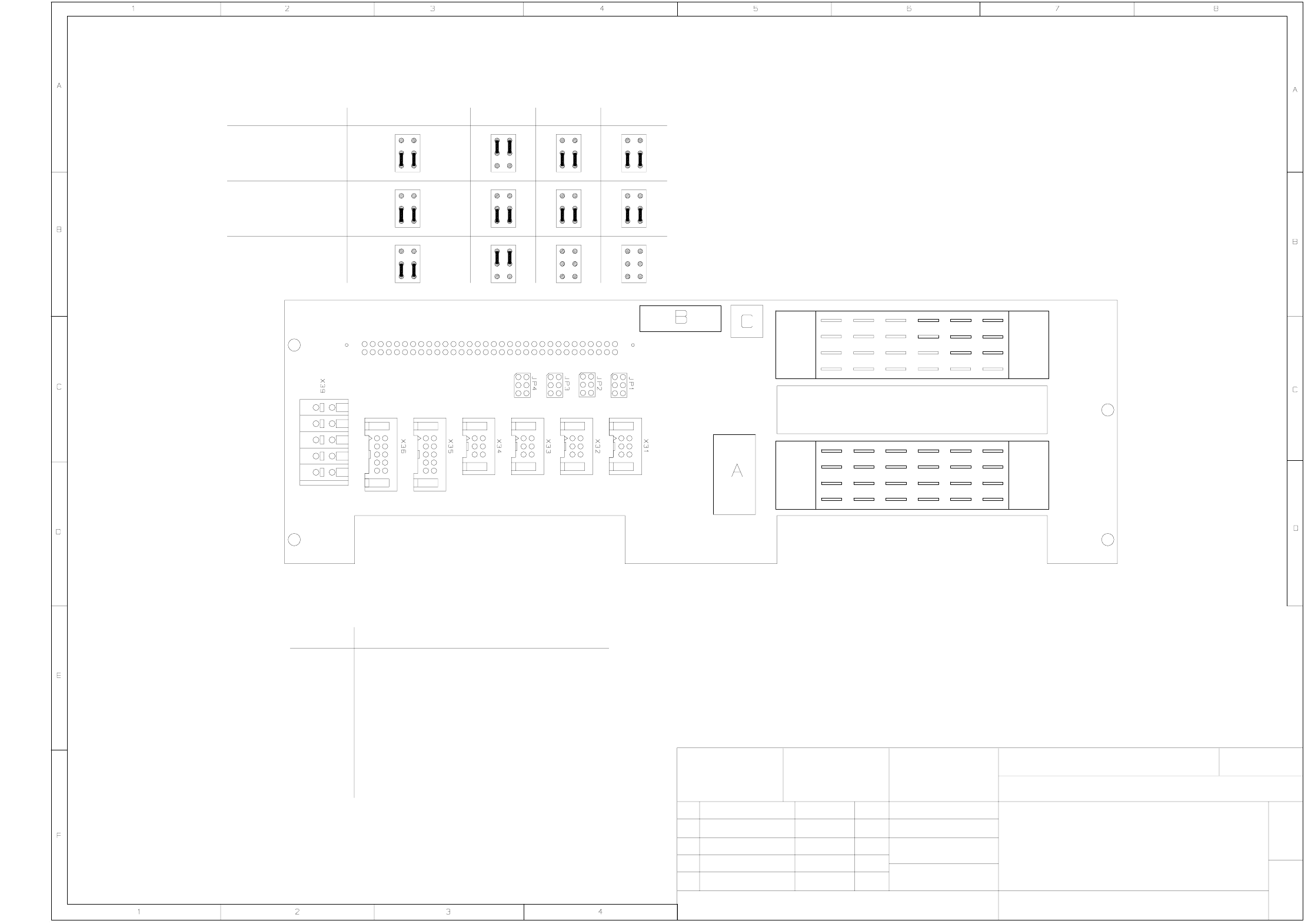
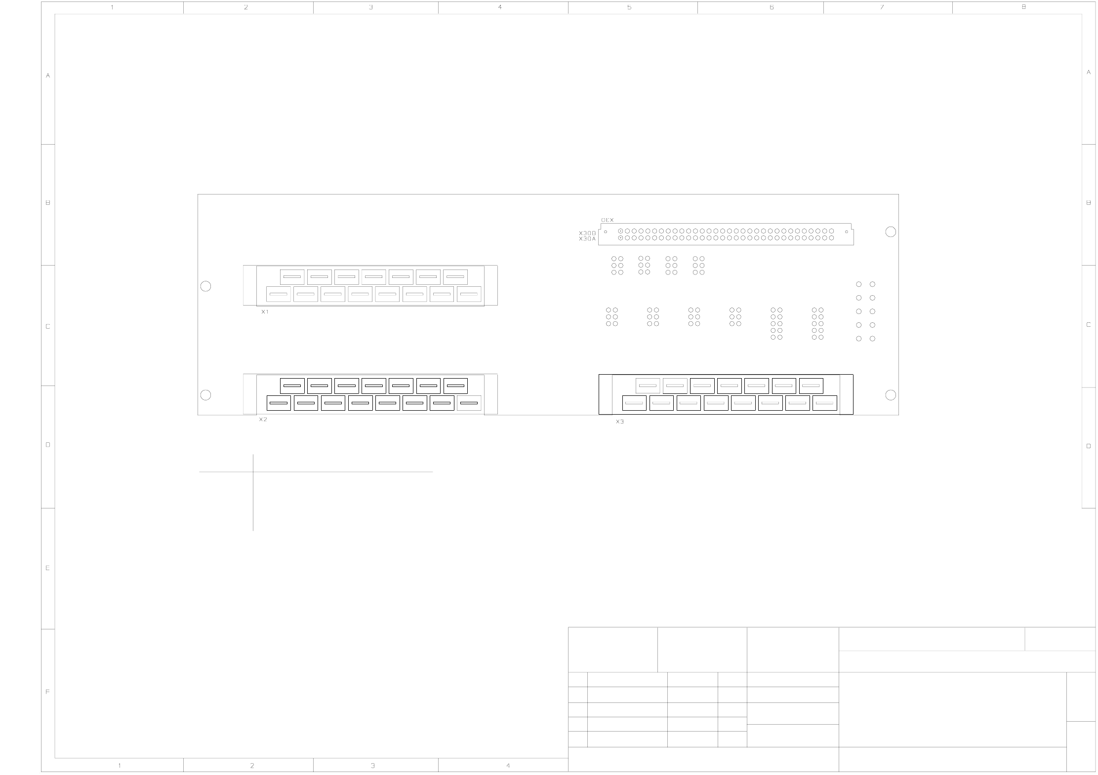
X4
X5
X31
X32
X33
X34
X35
X36
X39
X4
X5
1234 1234
a
b
c
d
e
f
e
d
c
b
a
54321
Plug
To servo backplanes
Crash signal, carrier cable interface
Crash signal, interface
Crash signal, carrier cable interface
Y1 (HF), Y1 (HF/3) crash signal
X2 (HF), X3 (HF/3), X4 (HF/3) crash signal
Y2 (HF), Y3 (HF/3), Y4 (HF/3) crash signal
X1 (HF), X1 (HF/3) crash signal
To servo backplanes
pflichten zu Schadenersatz. Alle Rechte vorbehalten, ins
besondere für den Fall der Patenterteilung oder GM-Eintragung
wertung und Mitteilung ihres Inhalts nicht gestattet, soweit
Weitergabe sowie Vervielfältigung dieser Unterlage,Ver-
nicht ausdrücklich zugestanden. Zuwiderhandlungen ver-
Proprietary date, company confidential. All rights reserved.
Confie a titre de secret d'entreprise. Tous droits reserves.
Confiado como secrete industrial. Nos reservamos todos los derechos.
Comunicado como segredo empresarial. Reservados todos os direitos.
HF/3 - P1+P4
HF/3 - P3
HF
JP4 JP2JP3 JP1
5 - 26
00353486-010401ND3 Anti-crash backplane / ballast circuit (Sh. 2 of 2)
00353486-010401ND3
Backplane anticrash / ballast circuit
1 : 1
Component layout, solder side
G32918 - N0037 - U021 - * - 17
KD
Name
KD
KD
KD
ModifiedStat.
01.
02.
03.
04.
30.08.01
27.04.01
Date
18.02.02
06.11.02 27.04.01
2-layer PCB
SIEMENS AG
Name
MCH2
I&S IS
Dorfner
Date
PC board
Scale
989
2 -
Sheet
pflichten zu Schadenersatz. Alle Rechte vorbehalten, ins
besondere für den Fall der Patenterteilung oder GM-Eintragung
wertung und Mitteilung ihres Inhalts nicht gestattet, soweit
Weitergabe sowie Vervielfältigung dieser Unterlage,Ver-
nicht ausdrücklich zugestanden. Zuwiderhandlungen ver-
Proprietary date, company confidential. All rights reserved.
Confie a titre de secret d'entreprise. Tous droits reserves.
Confiado como secrete industrial. Nos reservamos todos los derechos.
Comunicado como segredo empresarial. Reservados todos os direitos.
Ballast circuit (A19)
DC/DC converter +5V/15A (A17)X2
DC/DC converter ±15V (A18)
Anti-crash board (A20)X30
X3
Plug
X1
4
32
4
32
4
32