m220_383_02_process_manual工艺手册.pdf.pdf - 第46页
PROCESS DESCRIPTION P ROCESS M ANU AL 4.2-1 4.2 Flat Polycrystalline Si from SiH 4 4.2.1 Basic configuration SiH 4 Temperature f lat 610 o C (fine grain) 650 o C (coarse grain) 4.2.2 Description 4.2.2.1 Purpose A flat po…
PROCESS DESCRIPTION
P
ROCESS MANUAL
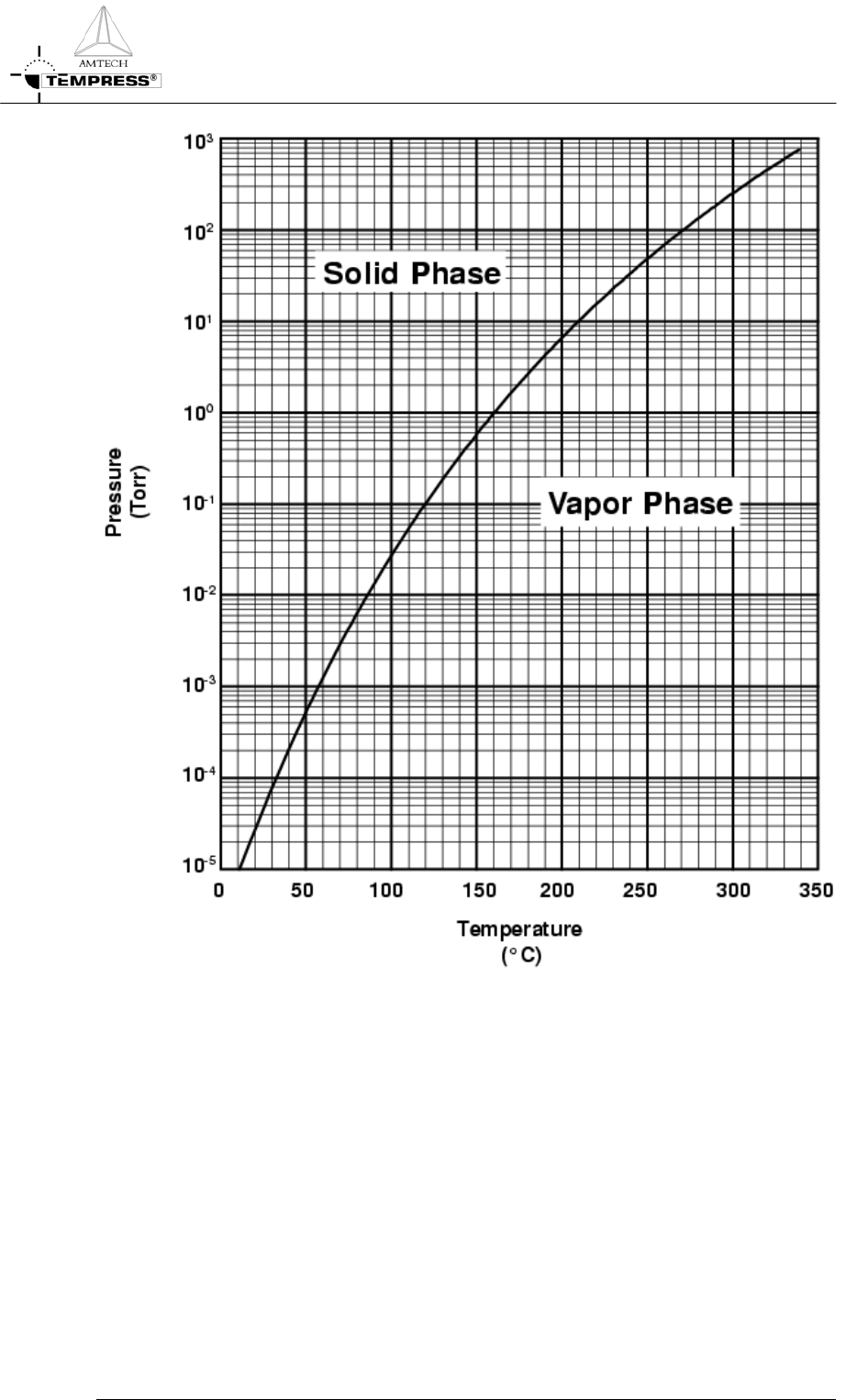
Figure 1: NH
4
Cl vapor pressure
4.1-10

PROCESS DESCRIPTION
P
ROCESS MANUAL
4.2-1
4.2 Flat Polycrystalline Si from SiH
4
4.2.1 Basic configuration
SiH
4
Temperature flat
610
o
C (fine grain)
650
o
C (coarse grain)
4.2.2
Description
4.2.2.1 Purpose
A flat poly-Si process is used in situations with a strong demand for exactly dimensioned
grain structures. As diffusion source it is required to have small grains (more grain boundaries
to diffuse along) and as “bulk material” in Thin Film Transistor (TFT) applications the grain
structure is involved in the mobility of charge carriers (larger grain means less grain
boundaries, less barriers to cross for the charge carriers and a higher mobility).
4.2.2.2 Chemicals
SiH
4
is a pyrogenic gas, which means it will burn spontaneously when it comes into contact
with O
2
or air. It is also toxic, but generally it will burn before it gets toxic.
4.2.2.3 Process
Since the temperature is flat and the reaction consumes SiH
4
(depletion) the thickness
decreases along the load.
This can be improved in basically two manners: by using a high flow of (inert) gases to dilute
the SiH
4
and reduce its consumption. This will affect the growth rate since the partial
pressure of SiH
4
is reduced. Or, use a specially designed set of injectors to create a
homogeneous local SiH
4
concentration. This latter approach is described in the next section.
Cross-wafer uniformity is generally pretty good, since the deposition process is limited by the
surface reaction part. A decreasing process pressure does improve the uniformity, both the
cross wafer and the cross load. If relatively small wafers are used compared to the tube
diameter an increased gas flow improves cross-wafer and cross-load uniformity drastically.
4.2.2.4 Typicalities
To improve cross-wafer uniformity of the edge wafers it is necessary to apply a set of dummy
wafers at the gas inlet side of the load. An extra boat might be necessary.
The injector design is crucial and consists of a tube with front- and back-flange, through
which one long double-sided injector is placed. An extra injector position is available to add
some extra SiH
4
at a specific position should that be required.
PROCESS DESCRIPTION
P
ROCESS MANUAL
4.2.3
Process result indication
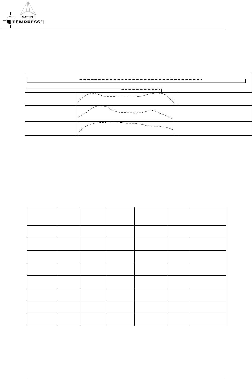
A schematic view of the thickness profile along the load as function of normalized gasflows is
given in the figure below.
Door Pump
A sccm
A sccm
Saddle profile
B sccm
C sccm
D sccm
F sccm
E sccm
The extra injector can also be removed to simplify processing.
4.2.4
Startup parameters for processing
The optical properties of a new and/or cleaned quartz tube change most dramatically after
the first deposition of foreign (=different refractive index) material. For accurate temperature
control a new and/or cleaned tube needs therefore to be coated before any (automatic)
profiling is performed. Use the default process settings for 1 hour to obtain a reasonable
coating.
An oxidized substrate wafer is required to enable accurate measurement, typically 1000Å
thermally oxidized wafers are used.
Type Wafer
Size
[mm]
Process
Time
[min]
Pressure
[mtor]
Thickness
[Å]
Temp.
[
o
C]
SiH
4
[sccm]
TS630x 100
150
30 250 3000 610 30-30-10
TS660x 100
150
30 250 3000 610 40-40-20
TS680x 100
150
30 250 3000 610 60-60-30
TS6100x 100
150
30 250 3000 610 60-60-30
TS840x 150
200
30 250 3000 610 60-60-30
TS860x 150
200
30 250 3000 610 80-80-40
TS8100x 150
200
30 250 3000 610 100-100-50
TS1280x 200
300
30 250 3000 610 200-150-50
4.2.5
Recommended cleaning interval
Cleaning interval for the several components after cumulative deposition in microns on the
wafers.
4.2-2