KE2040Instruction Manual Ver2.01,REV04.2003.6.25.pdf - 第33页
1 − 16 (2) Applicable component (For VCS r ecognit ion) Table 1-1-6-2 Item Par tial recognition Divided im age recognition Lead pitch Ball pitch Ball diameter Reflective Mi ni mum: 3 mm x 3 mm Ma ximu m: 50 m m x 50 mm M…
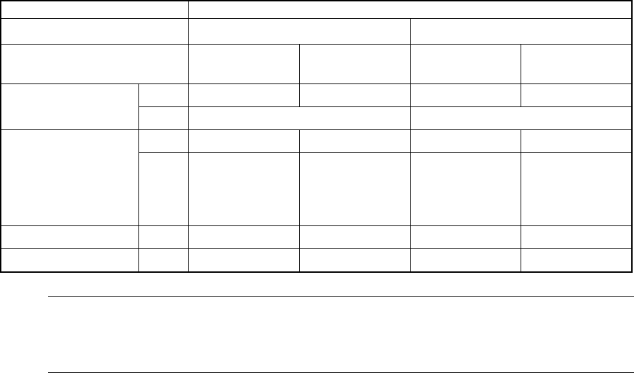
1 − 15
1.1.6 Applicable components and packages
(1) Applicable component sizes (For laser recognition with a KE-2020 only)
Table 1-1-6-1
Item Specifications
Component height specifications 12mm
20 mm (option at the factory)
Head Laser recognition
(MNLA)
Laser recognition
(FMLA)
Laser recognition
(MNLA)
Laser recognition
(FMLA)
Min. 0.2 mm
0.3 mm 0.2 mm
0.3 mm Component height
Max. 12 mm 20 mm
Min. 0.6 mm x 0.3 mm
1.0 mm x 0.5 mm
0.6 mm x 0.3 mm
1.0 mm x 0.5 mm
Component size
(Length x Width)
Max. 20 mm x 20 mm
or
26.5 mm x 11 mm
33.5 mm x 33.5 mm
or
Length of a diagonal
line: 47 mm
20 mm x 20 mm
or
26.5 mm x 11 mm
33.5 mm x 33.5 mm
or
Length of a diagonal
line: 47 mm
Lead pitch Min. 0.65 mm
0.65 mm
0.65 mm
0.65 mm
Ball pitch Min. 1.0 mm 1.0 mm 1.0 mm 1.0 mm
Note:
Four nozzles can pick up components whose size is 10 mm x 10 mm or less
simultaneously.
Two nozzles (No. 1 and 3 or No. 2 and 4: one nozzle is skipped) can pick up
components whose size is larger than 10 mm x 10 mm simultaneously.
1 − 16
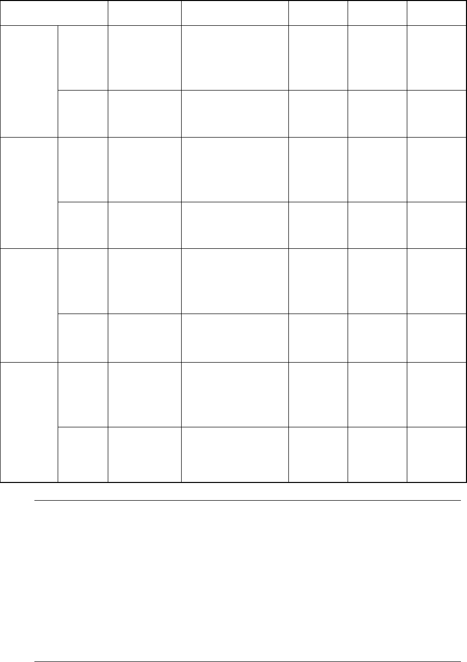
(2) Applicable component (For VCS recognition)
Table 1-1-6-2
Item Partial
recognition
Divided image
recognition
Lead pitch Ball pitch Ball
diameter
Reflective
Minimum:
3 mm x 3 mm
Maximum:
50 mm x 50 mm
Maximum:
50 mm x 150 mm
(when divided into 1 x 3)
Maximum:
74 mm x 74 mm
(when divided into 2 x 2)
Minimum:
0.38 mm
Maximum:
2.54 mm
Minimum:
1.0 mm
Maximum:
3.0 mm
Minimum:
φ 0.4mm
Maximum:
φ 1.0mm
Standard
VCS
(field of view:
54 mm)
Penetrative
Minimum:
9 mm x 9 mm
Maximum:
50 mm x 35 mm
Maximum:
35 mm x 120 mm
(when divided into 1 x 3)
Reflective
Minimum:
3 mm x 3 mm
Maximum:
34 mm x 34 mm
Maximum:
34 mm x 120 mm
(when divided into 1 x 3)
Maximum:
68 mm x 68 mm
(when divided into 2 x 2)
Minimum:
0.3 mm
Maximum:
2.54 mm
Minimum:
0.7 mm
Maximum:
2.0 mm
Minimum:
φ 0.28mm
Maximum:
φ 0.63mm
Optional
VCS-1
(field of view:
37.5 mm)
Penetrative
Minimum:
9 mm x 9 mm
Maximum:
34 mm x 34 mm
Reflective
Minimum:
3 mm x 3 mm
Maximum:
24 mm x 24 mm
Maximum:
24 mm x 72 mm
(when divided into 1 x 3)
Maximum:
48 mm x 48 mm
(when divided into 2 x 2)
Minimum:
0.3 mm
Maximum:
2.54 mm
Minimum:
0.5 mm
Maximum:
2.0 mm
Minimum:
φ 0.2mm
Maximum:
φ 0.63mm
Optional
VCS-2
(field of view:
27 mm)
Penetrative
Minimum:
9 mm x 9 mm
Maximum:
24 mm x 24 mm
Reflective
Minimum:
3 mm x 3 mm
Maximum:
15.5 mm x 15.5
mm
Maximum:
15.5 mm x 46.5 mm
(when divided into 1 x 3)
Maximum:
31 mm x 31 mm
(when divided into 2 x 2)
Minimum:
0.3 mm
Maximum:
2.54 mm
Minimum:
0.35 mm
Maximum:
2.0 mm
Minimum:
φ 0.14mm
Maximum:
φ 0.63mm
Optional
VCS-3
(field of view:
18 mm)
Penetrative
Minimum:
9 mm x 9 mm
Maximum:
15.5 mm x 15.5
mm
Note:
1. The minimum dimensions of a component to be recognized with the VCS are
applied only to a component whose mold dimensions are 7 mm x 7 mm or more.
2. The maximum dimensions of a component to be recognized with the standard
VCS should be within the recognizable range: 52 mm x 52 mm including a
component placement position error and a teaching error which is caused when
the machine picks up the component.
3. The center position of a component should be
±
1 mm or less (in the X and Y
direction) far from the camera center position and the component angle should
be
±
3
°
against the camera center position when the camera is recognizing the
component.
1 − 17
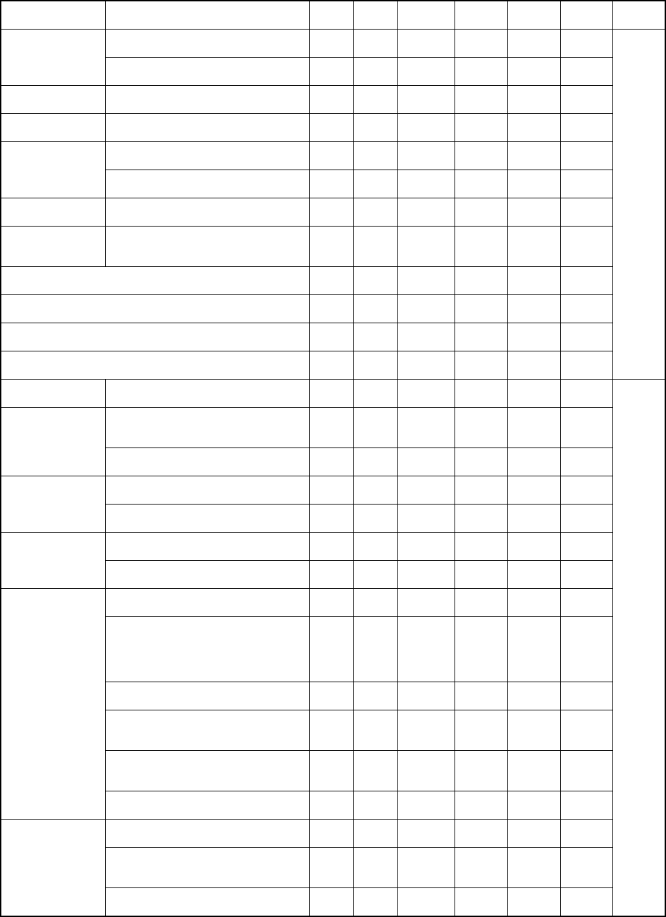
(3) Applicable component
Component
Name
Shape
MNLA
*1
FMLA Standard
VCS
Optional
VCS-1
Optional
VCS-2
Optional
VCS-3
Package
0603
○
Square chip
resistor
1005, 1608, 2012, 3216, 3225
(5025, 6432)
○
○
Network resistor (Excluding SOP, SOJ, PLCC types)
○
○
MELF resistor 1.6 x φ1.0mm, 2.0 x φ1.25mm, 3.5 x
φ1.4mm, 5.9 x φ2.2 mm
○
○
0603
○
○
Laminated
ceramic capacitor
1005, 1608, 2012, 3216, 3225, 4532,
5750 (5632)
○
○
Tantalum chip
capacitor
3216, 3528, 6032, 7343
○ ○
Aluminum
electrolytic
capacitor Height:
Height: more than 6 mm, but 10.5
mm or less
○
○ ○
Chip film capacitor
○
○
Variable trimmer capacitor, Chip potentiometer, trimmer
○
○
Chip ferrite beads
○
○
Chip inductor
○
○
Tape
SOT molded part 1608/2012, SOT-23,
SOT-89, SOT-143, SOT-223
○
○
8-, 14-, 16-, 18-, 20-, 24- and 28-pins
Length of a diagonal line: 31.5 mm or
less
○ ○ ○
SOP
32, 40-pin
○ ○
16, 18, 20, 24, 26, 28, 32-pin
○
○ ○
SOJ
40-pin
○ ○
18, 20, 22, 28 (Square),
28 (Rectangle), 32, 44-pins
○
○ ○
PLCC
52, 68, 84-pins
○ ○
Pitch 0.65/0.8/1.0
Dimensions: 20 mm x 20 mm or less
○
○ ○
Pitch: 0.65/0.8/1.0
Dimensions: more than 20 mm x 20
mm or 23.5 mm (length) x 11 mm
(width), but 33.5 mm x 33.5 mm or
less
○ ○
Pitch: 0.4/0.5/0.6/0.8/1.0
Dimensions: 50 mm x 50 mm or less
○
Pitch: 0.3
Dimensions: more than 24 mm x 24
mm, but 33.5 mm x 33.5 mm or less
○
Pitch: 0.3
Dimensions: more than 16 mm x 16
mm, but 24 mm x 24 mm or less
○ ○
QFP, BQFP
Pitch: 0.3
Dimensions: 16 mm x 16 mm or less
○ ○ ○
Dimensions: 20 mm x 20 mm or
less , 23.5 mm(L) x 11 mm(W) or less
○
○ ○
Dimensions: 20 mm x 20 mm , more
than 23.5 mm(L) x 11 mm(W), but
33.5 mm x 33.5 mm or less
○ ○
BGA
Dimensions: more than 33.5 mm x
33.5 mm, but 50 mm x 50 mm or less
○
Tape
Stick
Tray
*1 : applicable to a KE-2020
Table 1-1-6-3