KE2010.Instruction Manual.Ver.2.01,Rev.08.pdf - 第153页
4 – 46 165 125 10 10 ② Ref . hole pos. (Ref erence hole position) Enter the coor dinates of the positioning hole viewed from the PW B ref erence position in the same m anner as when you select “Single PW B” as the PW B c…
4 – 45
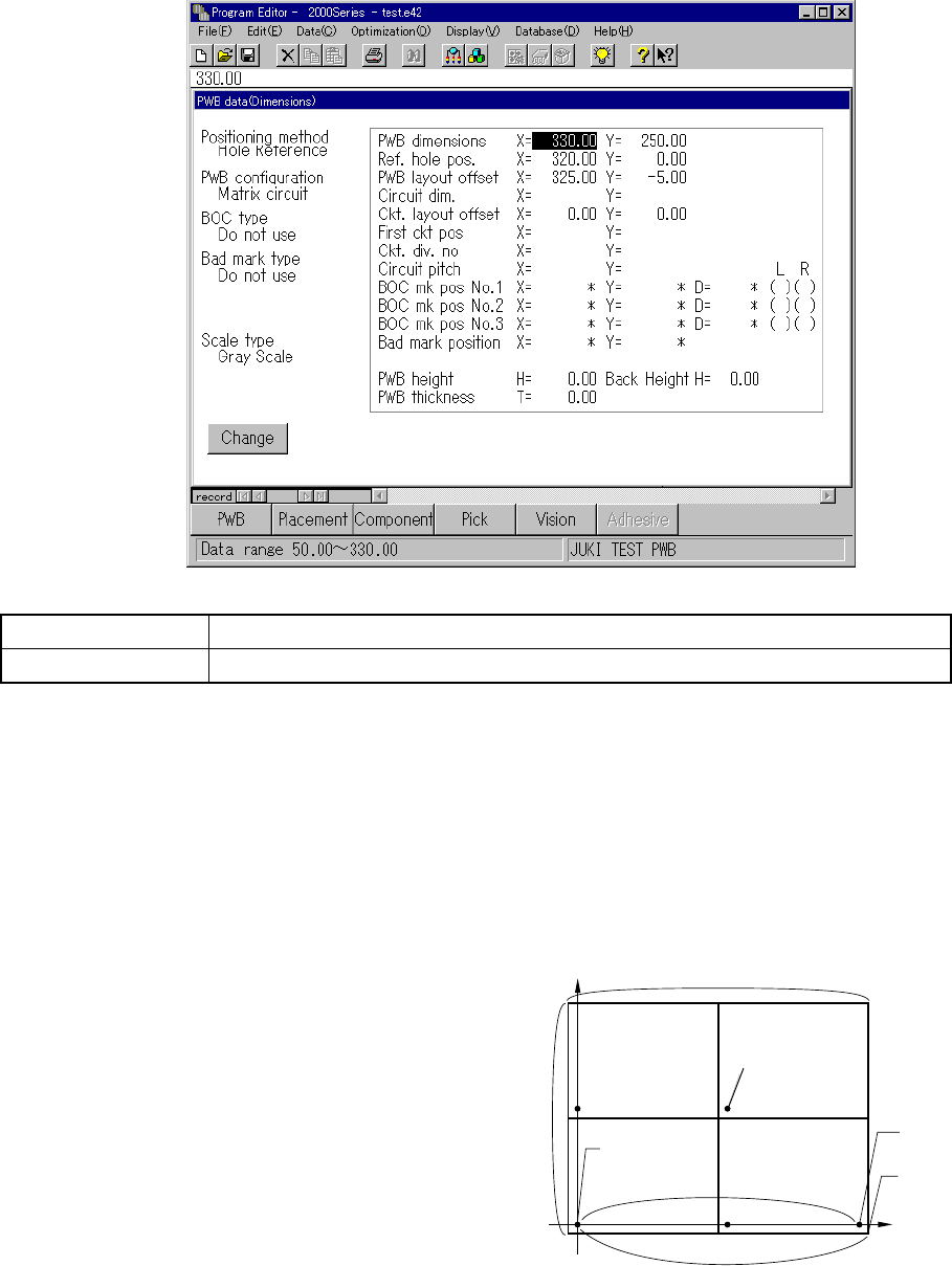
4.5.2.2 Matrix circuits patterns
When you select “Matrix circuit” as the PWB configuration and click the
<Dimension> button, a screen shown below appears.
Button Description
Change Displays the Basic setup change screen.
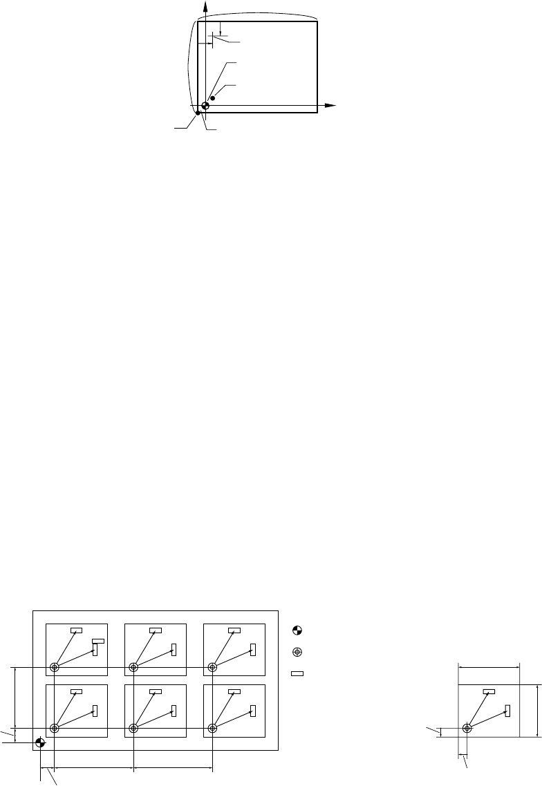
Before entering each dimension on the "Dimensions" column, be sure to set the
origin of each dimension. For a multiple pattern board, set the origin of a board
and that of a circuit separately (however, you may set the same point as the origin of
a board and that of a circuit). Since the origin specified in Placement data
becomes that of a circuit, we recommend that you specify the origin used in CAD
data as the origin of a circuit when you are to create Placement data from CAD data.
① PWB dimensions
Enter the outer dimensions of a
PWB in the same manner as
when you select “Single PWB” as
the PWB configuration.
X indicates the same direction as
the board transport direction,
while Y indicates the direction
perpendicular to the board
transport direction.
X = 330.00 Y = 250.00
250
330
(320, 0)
(325, -5)
Circuit reference
position
Reference pin
PWB layout
end point
PWB reference
position (origin)
4 – 46
165
125
10
10
② Ref. hole pos. (Reference hole position)
Enter the coordinates of the positioning hole viewed from the PWB reference
position in the same manner as when you select “Single PWB” as the PWB
configuration with assuming that the PWB reference position is the origin (0, 0).
Note that the reference hole position varies according to the board transport
direction or reference side: front or rear (see Figure 4.5.2.1). When you
select "Shape Reference" at the item "Positioning method" on the Basic setting
window, you do not have to enter any data here.
X = 320.00 Y = 0.00
③ PWB layout offset
Enter the coordinates of the PWB layout end point (that is, shape reference
position) viewed from the PWB reference position in the same manner as when
you select “Single PWB” as the PWB configuration.
Note that the PWB layout end point varies according to the board transport
direction and/or board transport reference side
X = 325.00 Y = - 5.00
④ Circuit dim. (dimension)
Enter the outer dimensions of a circuit.
X indicates the same direction as the board transport direction, while Y
indicates the direction perpendicular to the board transport direction.
X = 165.00 Y = 125.00
Figure 4.5.2.2 Matrix circuits drawing
⑤ Ckt. (Circuit) layout offset
Enter the coordinates of the circuit layout end point (that is, front left corner of a
circuit) viewed from the circuit reference position.
The circuit layout end point is fixed at the lower left corner of the PWB.
X = - 5.00 Y = - 5.00
BOC mark
Circuit reference position (0, 0)
Bad mark
Circuit layout end
it
Circuit layout offset (-5, -5)
Circuit
pitch Y
First circuit
position Y
PWB reference position
Circuit reference position
Component
Circuit layout
offset Y
Circuit
dimension X
Circuit
dimension Y
Circuit layout
offset X
4 – 47
⑥ First ckt. pos (circuit position)
Enter the coordinates of the circuit reference position of the first circuit (circuits
at the left front of a PWB) viewed from the PWB reference position.
(See Figure 4.5.2.2.)
X = 0.00 Y = 0.00
⑦ Ckt. div. no (Circuit division number)
Enter the number of circuits: X is the number of circuits located in the same
direction as the board transport direction, and Y is the number of circuits located
in the direction perpendicular to the board transport direction.
X = 2 Y = 2
⑧ Circuit pitch
Enter the circuit pitch: distance between the origins of two consecutive circuits:
X is the distance between two circuits located in the same direction as the
board transport direction, and Y is the distance in the direction perpendicular to
the board transport direction. (See Figure 4.5.2.2.)
X = 165.00 Y = 125.00
⑨ BOC mk pos (mark position) No. 1 to No. 3
When you select "PWB mark used" as the BOC type on the Basic setup window,
enter the distance from the PWB reference position to the center point of the
BOC mark.
When you select "Ckt. mark is used" as the BOC type on the Basic setup
window, enter the distance from the circuit reference position to the center point
of the BOC mark.
You can select two or three BOC marks. When you use three BOC marks, you
can use any of three BOC marks.
When using two BOC marks, select the two BOC marks which are placed
diagonally on the PWB. The position of the BOC mark can be taught.
An asterisk mark (*) in the parentheses is used to indicate the data completion
status.
For a user-designated template, "T" appears in the parentheses after the
system teaches the right station (see Section 5.4 "Teaching a Mark").
⑩ Bad mark position
Enter the bad mark position viewed from the circuit reference position.
A bad mark can be taught also. See Section 7.2.2.15 " Bad mark sensor
teaching ".
⑪ PWB height
If the height of the side on which a component is to be placed when a board is
clamped with a jig or like is different from that obtained when a flat board is
clamped, enter the difference with assuming that the height of the clamped flat
board upper side is 0.
The "+" sign indicates the up direction, while the "" sign does the down direction.
Since you cannot set the height of a board for each circuit, the height of each
circuit should be the same if you are to create a jig.
Normally, set this item to "0.00".