KE2010.Instruction Manual.Ver.2.01,Rev.08.pdf - 第37页
1 − 20 (5) Allow able height of a com ponent to be placed and allowable height of t he rear of a board Figure 1.1.7. 1 Component height speci fication Component height (mm) SC specif ication 6 HC specif ication 20 5. Boa…
1 − 19
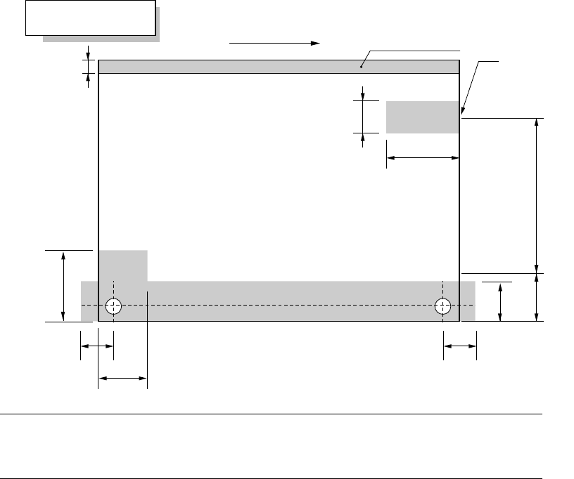
(4) Area in which backup pins cannot be proved KE-2010E
20mm
21mm
37mm
0mm ~220mm
4mm
50mm
17.5mm
36mm
17.5mm
105mm
Note: When the PWB is transferred from right to left, the marginal area of 50mm x
20mm is set on the left.
When the PWB is transferred from right to left, the marginal area of 36mm x
105mm is set on the right.
Movement of PWB
Conveying rail (fixed)
Area in which backup
pins cannot be provided
(Variable)
(35 mm when the PWB is transferred from right to left)
Stopper position
Extra large size
board s
p
ecifications
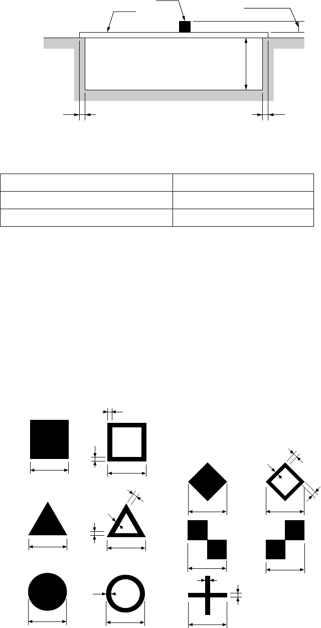
1 − 20
(5) Allowable height of a component to be placed and allowable height of the rear of
a board
Figure 1.1.7.1
Component height specification Component height (mm)
SC specification 6
HC specification 20
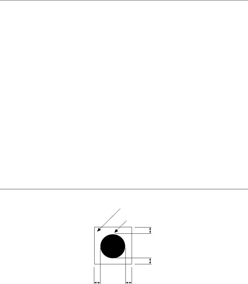
5. Board Recognition Marks
Create the board recognition marks under the following conditions. (See Figure
1.1.7.2.) We recommend the filled circle for the mark. The clearance area
around the mark shall be as shown in Figure 1.1.7.3. Within this area, there
shall not be any silk patterns, strip lines (including inner layer patterns), through
holes, resists, and other components.
A size: 0.5 to 3.0mm ±10
B size: 0.2 mm or more
C size: 0.5 to 3.0 mm ±10
A
B
B
B
A
A
A
C
B
C
C
C
C
A
B
A
B
B
B
B
B
B
Figure 1.1.7.2
Component
PWB
Max. 6 mm (SC specification)
Max. 20 mm (HC specification)
Marginal area
on the back no plecement
of PWB
(
see 3mm
)
Max.
40m
3 3
1 − 21
Notes: 1. When recognition, the mark shall be placed in the angle shown above.
However, if you specify "Use of each circuit mark" for a non-matrix PWB,
the mark can be recognized only when all marks of the reference circuit
are positioned in the angle described and the circuit is positioned at 90,
180, 270 or 360 degrees.
2. The fiducials of the same shape and same size is preferable within a
board.
3. When processing, copper foil or solder plating can be recognized.
4. Maximum number of marks which can be registered
Board mark: 1 set (2 marks or 3 marks)
IC mark: 50 sets (Pairs of 2 marks)
5. Items that can be registered
Mark number
Balance detection window
Normal/reverse rotation identification when detected
Mark shape
Outer dimensions
Effective value of projection
Matching
6. If there is no recognition mark on a board, register a user designated
template to allow the machine to recognize marks.
Figure 1.1.7.3
Clearance area
Recognition mark
0.5 mm or more mark
0.5 mm or more mark
0.5 mm or more mark