ED-7306_E.pdf - 第14页
JEITA ED-7306 - 12 - 3.3 Open solder joints after BGA board lev el assembly Take BGA as an example, since it indicates large r warpage at elevated temperature. Th e behaviors of the package warpage and the solder pa ste …
JEITA ED-7306
- 11 -
3. Brief contents of deliberations
3.1 Measurement methods of the package warpage at elevated temperature
The task force reached an agreement on the following facts after reviewing the experimental data from
member companies:
- The absorption of moisture increases the magnitude of the warpage.
- There is stronger correlation of the magnitude of the warpage with the temperature rather than the
temperature profile including duration of heat stress or temperature ramp rate. Also if the temperature
profile in the measurement simulates the reflow temperature profile forcibly, high temperature ramp rate
may cause temperature overshoot or larger temperature difference between the top and bottom sides of
the package, which makes the measurement inconsistent. Therefore, the approximation of the
temperature profile to the reflow condition is not a high priority.
- The warpage data of remeasurement are usually consistent, but some reports claimed poor
reproducibility in remeasurement. Therefore, the repetition of the measurement cycles to the same
sample is not recommended.
- Warpage data measured by the shadow moiré method agreed with those measured by the laser
reflection method as far as the measuring zone was the same.
- It was confirmed that zero to five hours in waiting time after pretreatment until measurement did not
show any difference in measurements.
Based on these agreements in facts, the measurement methods and conditions of package warpage at
elevated temperature were specified.
3.2 Maximum permissible package warpage at elevated temperature
This specification was initially drafted as a standard of the measurement method of the package warpage,
and their criteria were planned to be specified in each package design guide. However, the Subcommittee
decided to specify the maximum permissible package warpage of BGA, FBGA, and FLGA in this
specification. It is because the comprehensive specification provides the overall explanations for the budget
allocation of the maximum relative displacement and well-aligned criteria by ball pitch.
For stackable packages, the premise of the budget allocation, 80 % of the maximum relative displacement
to package and 20 % to PWB, is not valid; therefore, they are out of the scope in this specification.
The task force drafted the specification based on the theoretical approach to the mechanisms of open
solder joints and solder bridges, as well as the experimental approach to those through soldering the
artificially warped package. Maximum permissible package warpage of BGA is given 80 % of the maximum
relative displacement that does not cause open solder joints or solder bridges. The other 20 % of the
displacement is reserved for a tolerance of the PWB warpage and the fluctuation of the paste thickness.
On the other hand, the maximum permissible package warpage of FLGA is defined to be 100 % of the
maximum relative displacement. It is defined to be the height of the molten solder paste, which does not
cause open-solder joints. Any tolerance is reserved for the warpage of PWB because the maximum
permissible warpage is already very close to the coplanarity requirements. It implies how difficult mounting
FLGA is. There are some means to generate some extra tolerance to allow some PWB warpage, such as
thick pre-coated terminals to reserve some collapse height of FLGA during reflow.
This specification does not refer to such an extent.
JEITA ED-7306
- 12 -
3.3 Open solder joints after BGA board level assembly
Take BGA as an example, since it indicates larger warpage at elevated temperature. The behaviors of the
package warpage and the solder paste during the reflow process are described as follows:
(1) It is premised that the package is flat with acceptable coplanarity at room temperature and PWB is
ideally flat in all conditions.
(2) The package warps larger in association with rising temperature. Just below melting point, some
crowns of the solder balls may even separate from the surface of the solder paste at the package
corners, where the warpage is larger.
(3) As temperature rises further and exceeds the melting point of solder, the solder balls and paste melt
and collapse.
(4) Even if the crowns of some solder balls were apart from the solder paste just below the melting point,
the collapse of the balls produces good solder connection with the activated solder paste.
(5) Acceptable solder joints are formed after reflow.
(6) In case package warps more than the criteria, the crowns of these balls does not touch the paste
when the balls collapse. It causes the open solder joints.
Under the consideration of mechanisms from (1) to (6), if the sum of package warpage at elevated
temperature and the lowest standoff height is smaller than the sum of the original solder-ball height and the
thickness of the molten solder paste, good solder connection can be expected after the board assembly,
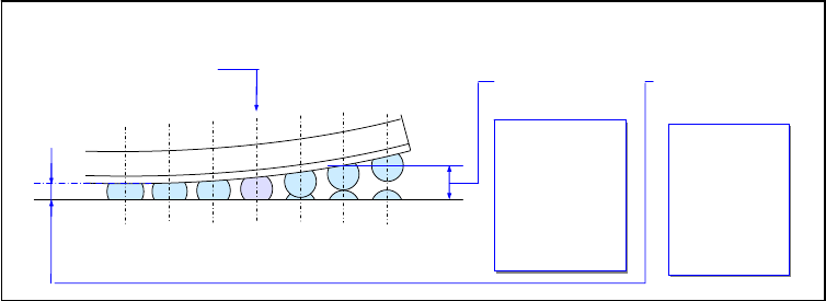
and vice versa. (See Explanatory Fig. 1)
The maximum relative displacement is defined as the difference between the highest and
the lowest solder joint heights of BGA package mounted on the ideally flat seating plane,
where none of solder joints are open.
Explanatory Fig. 1 Calculation of the maximum relative displacement immune
from open solder joints
Highest joint
height of BGA
without open
solder joints
Lowest joint
height of BGA
without open
solder joints
Original
solder ball
height
+
Molten
solder height
Original
solder ball
height
+
Molten
solder height
Nominal solder joint
height of ideally flat
package
Empirical
data
↓
Nominal
joint height
x 0.87
Empirical
data
↓
Nominal
joint height
x 0.87
Ideally flat seating plane
JEITA ED-7306
- 13 -
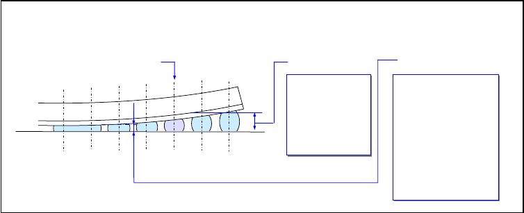
3.4 Solder ball bridges after BGA board level assembly
The occurrence of the solder ball bridges depends on how much package warps during reflow process. The
mechanisms of the solder ball bridges are described below:
(1) If the package warpage is less than the maximum permissible warpage just above the melting point,
all solder balls are once soldered to the lands on PWB.
(2) Further elevation of the temperature makes some balls flattened while others stretched because of
the increase in package warpage.
(3) The collapsed balls have larger diameters, while the stretched balls become thinner but are still
connecting the package and PWB owing to surface tension.
(4) When the diameters of the collapsed balls expand beyond the certain percentage of the ball pitch
(80 % of the ball pitch obtained from the experimental data), the failure rate of the short circuits
increases.
Therefore, the maximum relative displacement of the package without the solder bridge is the difference
between the height of the stretched balls (the highest joint height) and that of the flattened balls (the lowest
joint height) whose diameter is 80 % of the ball pitch. (See Explanatory Fig. 2)
The maximum relative displacement is defined as the difference between the highest and
the lowest joint heights of BGA package mounted on the ideally f lat seating plane, where
none of solder joints bridge.
NOTE: Constants of the calculations are obtained from the experiment and used for simplicity.
Explanatory Fig. 2 Calculation of the maximum relative displacement immune
from solder ball bridges
Highest ball
height of BGA
without solder
bridge.
Lowest ball
height of BGA
without solder
bridge.
Empirical
data
↓
Nominal joint
height x 1.3
Empirical
data
↓
Nominal joint
height x 1.3
Nominal joint height of
ideally flat package
Ball pitch>Ball
width
↓
Empirical data:
Pitch x 0.8
↓
Height
calculation
Ball pitch>Ball
width
↓
Empirical data:
Pitch x 0.8
↓
Height
calculation
Ideally flat
seating plane