ED-7306_E.pdf - 第18页
JEITA ED-7306 - 16 - 3.6 Maximum permissible package warpage of FLGA Given that PWB is an ideal seating plane, the maxi mum package warpage is defined to be the thickness of molten solder paste. (S ee Explanatory Fig. 3 …
JEITA ED-7306
- 15 -
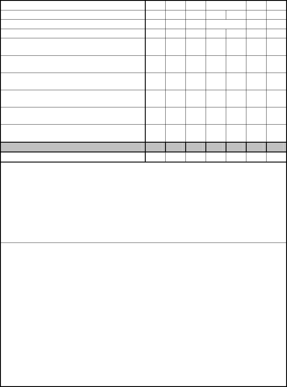
Explanatory Table 1 Maximum permissible package warpage for BGA and FBGA
Unit: mm
Solder ball pitch 0.4 0.5 0.65 0.8 1.0 1.27
Condition of solder ball height
a)
0.20 0.25 0.33 0.35 0.40 0.50 0.60
Condition of solder paste thickness after reflow
b)
0.08 0.10 0.11 0.13 0.14 0.15
Nominal solder joint height of the ideally flat package 0.18 0.23 0.29 0.31 0.36 0.43 0.5
Highest solder joint height of BGA without open
solder joint
c)
0.28 0.35 0.44 0.48 0.53 0.64 0.75
Lowest solder joint height of BGA without open
solder joint
d)
0.16 0.20 0.25 0.27 0.31 0.37 0.44
Highest solder joint height of BGA without solder
bridge
e)
0.24 0.29 0.38 0.40 0.46 0.55 0.66
Lowest solder joint height of BGA without solder
bridge
f)
0.12 0.15 0.20 0.19 0.25 0.28 0.34
Max relative displacement of BGA without open
solder joint
g)
0.12 0.15 0.19 0.21 0.22 0.27 0.31
Max relative displacement of BGA without solder
bridge
h)
0.12 0.14 0.18 0.21 0.21 0.28 0.32
Max permissible package warpage (Absolute value)
i)
0.10 0.11 0.14 0.17 0.17 0.22 0.25
Coplanarity at room temperature (For reference) 0.08 0.08 0.10 0.10 0.10 0.20 0.20
NOTE: Assumptions of the calculations are
• The structure of the lands on PWB is non solder mask defined;
• The diameter of the lands on PWB is the same as that of package;
• Solder joint height between package and PWB is the distance between the face-to-face copper
lands;
• Thicknesses of the metal masks for solder paste printings are
- 0.10 mm for 0.4 mm pitch FBGA,
- 0.12 mm for 0.5 mm and 0.65 mm pitch FBGA, and
- 0.15 mm for 0.8 mm, 1.0 mm, and 1.27 mm pitch BGA;
• Opening diameter of the solder printing mask is the same as that of the lands on PWB.
Table footnote:
a)
It follows the specification in JEITA EDR-7315 and JEITA EDR-7316.
b)
It is the thicknesses of molten solder paste on copper lands without any component attached,
supposed 50 % of solder paste is metal content (solder).
c)
It is the sum of the solder ball height and the molten solder-paste thickness, where the solder
connections are immune from open circuit.
d)
It is 87 % of the nominal standoff height of the ideally flat package. The ratio is obtained from the
empirical data taken from the intentionally concave-warped sample.
e)
It is 130 % of the nominal standoff height of the ideally flat package. The ratio is obtained from the
empirical data taken from the intentionally convex-warped sample.
f)
It is the sum of the molten solder and the solder ball height when the ball diameter expands to 80 % of
the ball pitch. It is known that the balls do not bridge as far as the collapse of solder balls does not
make the ball diameter expand beyond 80 % of the ball pitch.
g)
It is the difference between the highest and the lowest solder joint height, where open solder joint is
not seen.
h)
It is the difference between the highest and the lowest solder joint height, where solder ball bridge is
not seen.
i)
It is 80 % of the maximum relative displacement.
JEITA ED-7306
- 16 -
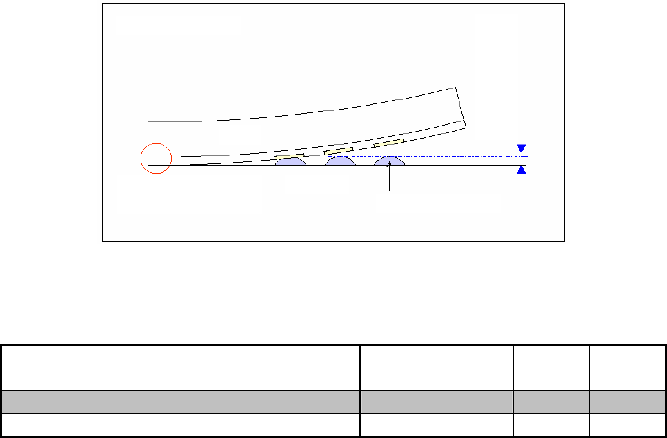
3.6 Maximum permissible package warpage of FLGA
Given that PWB is an ideal seating plane, the maximum package warpage is defined to be the thickness of
molten solder paste. (See Explanatory Fig. 3) However the maximum permissible package warpage
depends on the amount of the solder paste, the criteria for FLGA are specified in Explanatory Table 2 for
semiconductor suppliers.
Explanatory Fig. 3 Package warpage of FLGA at elevated temperatu
Explanatory Table 2 Maximum permissible package warpage for FLGA
Unit: mm
Land pitch 0.4 0.5 0.65 0.8
Condition of thickness of molten solder 0.08 0.10 0.11 0.13
Maximum permissible package warpage (Absolute value) 0.08 0.10 0.11 0.13
Coplanarity at room temperature (For reference) 0.08 0.08 0.10 0.10
3.7 Discussion with the TSC on Jisso Technology Standardization
After drafting this specification, the task force requested the TSC on Jisso Technology Standardization to
review this specification and to hold the joint ad hoc meeting to promote harmonization of the opinions
between suppliers and users. Most of the issues raised by TSC were corrected or added, but there were
some disagreements left. Chief request was to verify if the measurement data from different types of
instruments are well accorded with. With the collaboration of measuring instrument suppliers, the bimetal
samples were measured by 3 types of instruments.
Since the TSC on Jisso Technology Standardization did not have enough data to comment on the criteria of
the maximum permissible package warpages, they would review the criteria one year later after the
collection of the data of the package warpages and the board assembly yields.
4. Industry property rights
The task force surveyed the industrial property rights that directly related to the measurement methods and
the maximum permissible warpage but did not find any of them.
FLGA
Maximum permissible
package warpage at
elevated temperature
Molten solder paste
PWB
The lowest point where
FLGA settles on PWB.
FLGA warpage
JEITA ED-7306
- 17 -
5. Relation to the international standard
There is not any international standard (IEC) related to the warpage measurement method at elevated
temperature but the JESD22B112 published by JEDEC, USA. The comparisons between JESD22B112
and this specification are shown below:
Item
JESD22B112 This specification (JEITA)
Object Surface mount devices BGA, FBGA, FLGA, but excluding QFP
Warpage
direction
Convex warpage results in the package
corners being closer to the seating plane than
the center of the bottom surface of the
package. Concave warpage results in the
package corners being farther from the seating
plane than the center of the bottom surface of
the package.
Same as JESD22B112
Measuring
zone
Unspecified a) For the packages whose standoff height is
more than 0.1 mm, such as BGA and FBGA,
the measuring zone is the area where
terminals are located. This area is bordered
by the lines connecting the centers of the
outermost neighboring solder balls. If there
are thermal balls at the package center,
their area is also considered as a part of
measuring zones.
b)
For the packages whose standoff height is
0.1 mm or less, such as FLGA, the
measuring area is the substrate surface
except certain edge margin. The width of
this margin L depends on the capability of
each measuring instrument (0.2 mm
recommended).
Package
warpage sign
Convex warpage is plus.
Concave warpage is minus.
Plus or minus sign of package warpage
determined by the sign of the sum of the
largest positive displacement and the largest
negative displacement of the package profile
on both measurement zone diagonals.
Package
warpage
“Deviation from planarity” is the difference in
height between the highest point and the
lowest point on the package body bottom
surface measured with respect to the seating
plane.
The difference of the largest positive and the
largest negative displacements of the package
warpage in the measuring zone with respect to
the reference plane, preceded by package
warpage sign. This reference plane is derived
using the least square method with the
measuring zone data.
Measuring
instrument
Shadow moiré only The measurement methods of the package
warpage are shadow moiré or laser reflection
method.
Calibration Concave or convex ground glass made of
ultra-low expansion material
Unspecified
Measurement
points
Warpage measurements should be viewed on
the substrate side without solder balls
attached.
The measurement points shall not be on the
crown of solder balls but on the substrate
surface of the package. Only when the
behavior of the package top surface (mostly
marking surface) is verified to coincide with
that of the substrate surface, the measurement
from the top surface is allowed.