ED-7306_E.pdf - 第21页
JEITA ED-7306 - 19 - 6. Deliberation members The scheme of this standard was made by the S ubcommittee on Integrated Circuit Packag es and deliberated by the Task force of the package wa rpage measurement at elevated tem…
JEITA ED-7306
- 17 -
5. Relation to the international standard
There is not any international standard (IEC) related to the warpage measurement method at elevated
temperature but the JESD22B112 published by JEDEC, USA. The comparisons between JESD22B112
and this specification are shown below:
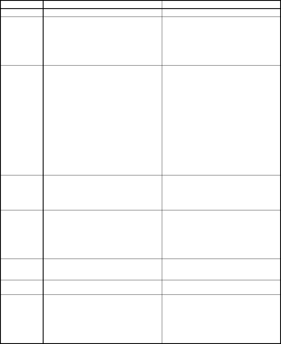
Item
JESD22B112 This specification (JEITA)
Object Surface mount devices BGA, FBGA, FLGA, but excluding QFP
Warpage
direction
Convex warpage results in the package
corners being closer to the seating plane than
the center of the bottom surface of the
package. Concave warpage results in the
package corners being farther from the seating
plane than the center of the bottom surface of
the package.
Same as JESD22B112
Measuring
zone
Unspecified a) For the packages whose standoff height is
more than 0.1 mm, such as BGA and FBGA,
the measuring zone is the area where
terminals are located. This area is bordered
by the lines connecting the centers of the
outermost neighboring solder balls. If there
are thermal balls at the package center,
their area is also considered as a part of
measuring zones.
b)
For the packages whose standoff height is
0.1 mm or less, such as FLGA, the
measuring area is the substrate surface
except certain edge margin. The width of
this margin L depends on the capability of
each measuring instrument (0.2 mm
recommended).
Package
warpage sign
Convex warpage is plus.
Concave warpage is minus.
Plus or minus sign of package warpage
determined by the sign of the sum of the
largest positive displacement and the largest
negative displacement of the package profile
on both measurement zone diagonals.
Package
warpage
“Deviation from planarity” is the difference in
height between the highest point and the
lowest point on the package body bottom
surface measured with respect to the seating
plane.
The difference of the largest positive and the
largest negative displacements of the package
warpage in the measuring zone with respect to
the reference plane, preceded by package
warpage sign. This reference plane is derived
using the least square method with the
measuring zone data.
Measuring
instrument
Shadow moiré only The measurement methods of the package
warpage are shadow moiré or laser reflection
method.
Calibration Concave or convex ground glass made of
ultra-low expansion material
Unspecified
Measurement
points
Warpage measurements should be viewed on
the substrate side without solder balls
attached.
The measurement points shall not be on the
crown of solder balls but on the substrate
surface of the package. Only when the
behavior of the package top surface (mostly
marking surface) is verified to coincide with
that of the substrate surface, the measurement
from the top surface is allowed.
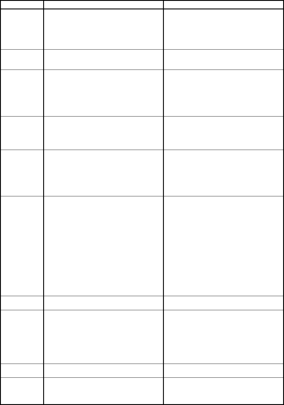
JEITA ED-7306
- 18 -
Item
JESD22B112 This specification (JEITA)
Solder ball
removal
• A simulated solder ball attachment process is
recommended to subject the test samples to
the same thermal exposure.
• Verification of the technique used to remove
the solder balls must be conducted.
• If the samples are prepared without solder
balls, they shall be subjected to the
simulated reflow profile.
• In the case of removal of the solder balls, it is
recommended to use mechanical removal
rather than hot reflow.
Peripheral lead
packages
For lead frame based packages, either the top
or bottom for the package body surface can be
measured.
Peripheral lead packages are excluded in the
scope of this specification.
Sample A minimum of 3 samples shall be measured to
determine variation within an assembly lot. It is
recommended that samples be measured in
both the moisture soaked and dry states.
If this test method is used for monitoring then
the package warpage may be measured in
only the dry state.
• Standard sample size is a minimum of 3
samples with pretreatment.
• The same sample shall not be subjected to
the repetition of the reflow profile cycles.
Pretreatment
of the samples
The minimum moisture soaked condition shall
be the rated moisture sensitivity level per
J-STD-020. It specifies that the waiting time
for the measurement after pretreatment shall
be 4 h or less.
Pretreatment conditions shall conform to
JEITA ED-4701/300 to measure the package
warpage.
Waiting time for measurement shall be no
longer than 5 hours after the pretreatment.
Thermocouple Thermocouple of gauge 30 or finer is
recommended. When polyimide tape is used,
it is recommended that a thermal paste should
be applied between the thermocouple bead
and the surface of the test sample. (Original
document quotes the commercial name for the
polyimide tape.)
A thermocouple of gauge 30 (φ0.25 mm) or flat
tip type is recommended.
When polyimide tape is used, a thermal sheet
is applied between the thermocouple bead and
the package surface.
Temperature
measurement
Ideally, a temperature ramp rate that can
closely match the reflow profile should be
used. The equipment should be configured to
achieve as fast a ramp rate as possible without
introducing significant delta temperature
differences between the top and bottom of the
package body.
The temperature profile of the warpage
measurement does not necessarily simulate
that for production. Higher priorities are placed
on
-
maintaining the temperature constant
during the measurement,
-
never exposing the samples unnecessary
duration to high temperature. Samples
shall be proceeded to the next
measurement as soon as possible,
-
avoiding temperature surge to prevent the
overshoot, and
-
minimizing the temperature difference
between the top surface and the substrate
surface.
Reflow oven Thermal chambers equipped with assisted
convective heating are highly recommended.
Unspecified
Data - A plot showing total warpage magnitude
versus temperature with the (+) and (-)
conventions assigned.
-
3-D contour plots of package shape as a
function of peak reflow temperature.
-
Diagonal line scans showing total warpage
magnitude across the diagonal of the
component.
• Temperature dependency of the package
warpage
• 3D plots of surface topography at each
temperature
• Diagonal profile of the package at each
temperature
Recommended
datasheet
Unspecified • Typical temperatures for measurement and
recommended datasheet are described.
Maximum
permissible
package
warpage
Unspecified • Maximum permissible package warpages for
BGA, FBGA, and FLGA are specified in this
specification.
JEITA ED-7306
- 19 -
6. Deliberation members
The scheme of this standard was made by the Subcommittee on Integrated Circuit Packages and
deliberated by the Task force of the package warpage measurement at elevated temperature.
The participated members are:
<Technical Standardization Committee on Semiconductor Device Packages>
TSC chair Chiaki Takubo Toshiba Corp.
<Subcommittee on Integrated Circuit Packages>
SC chair Hiroyuki Shigeta Sony Corp.
<Task force on package warpage measurement standardization at elevated temperature>
Leader Hirofumi Nakajima NEC Electronics Corp.
Member Koujiro Shibuya NEC Electronics Corp.
Akio Nakamura Oki Electric Industry Co., Ltd.
Hiroyuki Shigeta Sony Corp.
Hitoshi Shibue Sony Corp.
Yasuhiro Koshio Toshiba Corp.
Tsuyoshi Kanazawa Toshiba Corp.
Daisuke Otani Toshiba Corp.
Takayuki Maeda Texas Instruments Japan Ltd.
Kazunari Kosakai Fujitsu Ltd.
Takahiro Nakano Matsushita Electric Industrial Co., Ltd.
Takanori Hashizume Renesas Technology Corp.
Hiroshi Kawakubo Renesas Technology Corp.
Special members Tomoya Kiga Sony EMCS Corp.
Takanori Miyata Cermatronics Boeki Co., Ltd.
Nobuhiko Takahashi Hitachi Technologies and Services, Ltd.
Yoshio Ichikawa Cores Corp.